STM32F系列ARM Cortex-M3核微控制器基础之系统时钟一
2017-01-01 21:43
375 查看
STM32F系列ARM Cortex-M3核微控制器基础之系统时钟
本文章是基于STM32F103ZE微控制器,主要是详细说明STM32F系列的特性,由于本人是初学者,出现错误是难免的,请大家见谅。固件库采用V3.5.0版本
下面是STM32的时钟树


为使讲解更加清晰,我们把图分解开来,一部分一部分来看:
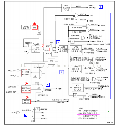
1、HSI高速内部时钟,RC振荡器,频率为8MHz。
2、HSE高速外部时钟,可接石英/陶瓷谐振器,或接外部时钟源,频率范围为4MHz~16MHz。
3、LSI低速内部时钟,RC振荡器,频率为40kHz。
4、LSE低速外部时钟,接频率为32.768kHz的石英晶体。
如果将时钟系统看作是一颗大树,那么1,2,3,4部分可以看作为树的根部。这里是时钟产生的地方,有关这部分的讲解后面会提到。
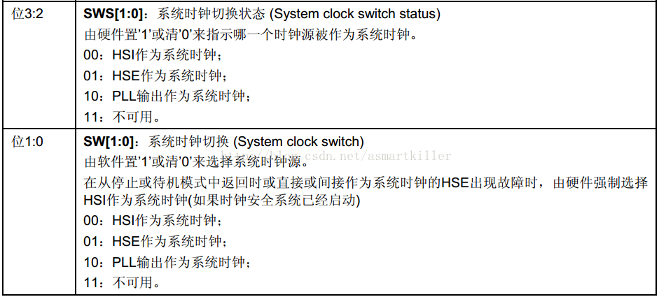
下面说的是时钟树的主要躯干部分: 图中的SYSCLK是系统时钟(最大为72MHz),有三种不同的时钟源可以用来驱动系统时钟:HSI振荡器时钟,HSE振荡器时钟,PLL时钟。这三个时钟源由SW确定。(SW是时钟配置寄存器RCC_CFGR中的第1:和0位:系统时钟切换 System clock switch)。系统复位后, HSI振荡器被选为系统时钟。当时钟源被直接或通过PLL间接作为系统时钟时,它将不能被停止。只有当目标时钟源准备就绪了(经过启动稳定阶段的延迟或PLL稳定),从一个时钟源到另一个时钟源的切换才会发生。在被选择时钟源没有就绪时,系统时钟的切换不会发生。直至目标时钟源就绪,才发生切换。在时钟控制寄存器(RCC_CR)里的状态位指示哪个时钟已经准备好了,哪个时钟目前被用作系统时钟。I2S音频总线时钟直接来源于系统时钟。
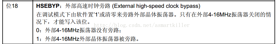
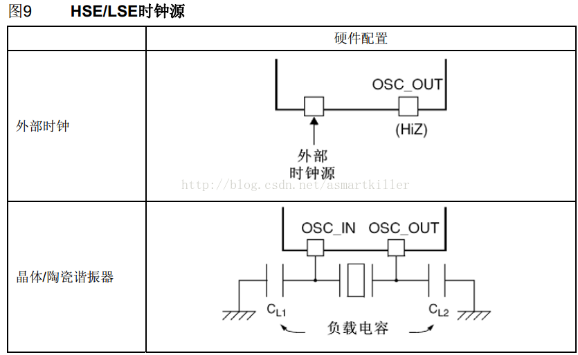
高速外部时钟信号HSE由两种时钟源产生,即HSE用户外部时钟(HSE旁路)和HSE外部晶体/陶瓷谐振器。
1.第一种模式:外部时钟源,它的频率最高可达25MHz。用户可以通过设置在时钟控制寄存器中的HSEBYP和HSEON位来选择这一模式。外部时钟信号(50%占空比的方波、正弦波或三角波)必须连接到SOC_IN引脚,同时保证OSC_OUT悬空。
2.第二种模式为外部晶体/陶瓷谐振器。在这种情况下需要等晶体振荡器稳定才能采用。
下面该图为这两种方式的硬件接法:这两种模式通过硬件配置和外部高速时钟旁路位来配置。
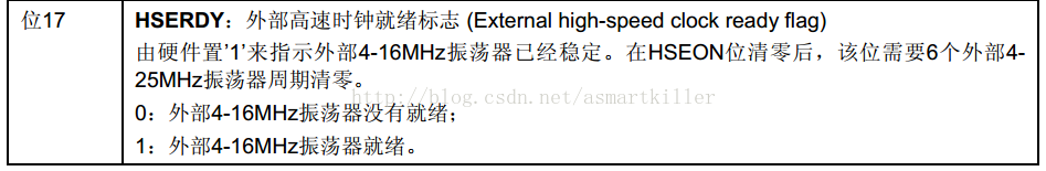
在时钟控制寄存器RCC_CR中的HSERDY位用来指示高速外部振荡器是否稳定。在启动时,直到这一位被硬件置’1’,时钟才被释放出来。如果在时钟中断寄存器RCC_CIR中允许产生中断,将会产生相应中断。HSE晶体可以通过设置时钟控制寄存器里RCC_CR中的HSEON位被启动和关闭。

高速外部时钟信号HSE可直接作为SYSCLK系统时钟(通过SW选择),也可以经过PLLXTPRE多路复用器选择直接或者二分频后输给PLLMUL倍频器后(RCC_PLLConfig函数中配置)作为系统时钟。

这里还有监控SYSCLK时钟的特性,该特性跟HSE振荡器有关:
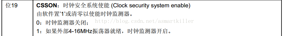
时钟安全系统(CSS):时钟安全系统可以通过软件被激活。一旦其被激活,时钟监测器将在HSE振荡器启动延迟后被使能,并在HSE时钟关闭后关闭。如果HSE时钟发生故障,HSE振荡器被自动关闭,时钟失效事件将被送到高级定时器(TIM1和TIM8)的刹车输入端,并产生时钟安全中断CSSI,允许软件完成营救操作。此CSSI中断连接到Cortex™-M3的NMI中断(不可屏蔽中断)。注意:
一旦CSS被激活,并且HSE时钟出现故障, CSS中断就产生,并且NMI也自动产生。 NMI将被不断执行,直到CSS中断挂起位被清除。因此,在NMI的处理程序中必须通过设置时钟中断寄存器(RCC_CIR)里的CSSC位来清除CSS中断。如果HSE振荡器被直接或间接地作为系统时钟,(间接的意思是:它被作为PLL输入时钟,并且PLL时钟被作为系统时钟),时钟故障将导致系统时钟自动切换到HSI振荡器,同时外部HSE振荡器被关闭。在时钟失效时,如果HSE振荡器时钟(被分频或未被分频)是用作系统时钟的PLL的输入时钟,PLL也将被关闭。
高速内部时钟信号HSI由内部8MHz的RC振荡器产生,可直接作为系统时钟或在2分频后作为PLL输入。当HSI被用于作为PLL时钟的输入时,系统时钟能得到的最大频率是64MHz。HSI RC振荡器能够在不需要任何外部器件的条件下提供系统时钟。它的启动时间比HSE晶体振荡器短。然而,即使在校准之后它的时钟频率精度仍较差。校准制造工艺决定了不同芯片的RC振荡器频率会不同,这就是为什么每个芯片的HSI时钟频率在出厂前已经被ST校准到1%(25°C)的原因。系统复位时,工厂校准值被装载到时钟控制寄存器的HSICAL[7:0]位。如果用户的应用基于不同的电压或环境温度,这将会影响RC振荡器的精度。可以通过时钟控制寄存器里的HSITRIM[4:0]位来调整HSI频率。时钟控制寄存器中的HSIRDY位用来指示HSI
RC振荡器是否稳定。在时钟启动过程中,直到这一位被硬件置’1’, HSI RC输出时钟才被释放。 HSI RC可由时钟控制寄存器中的HSION位来启动和关闭。如果HSE晶体振荡器失效, HSI时钟会被作为备用时钟源。
下面来看看时钟树躯干部分(即标号5处)的相关内容:
5.PLL可以用来倍频HSI RC的输出时钟或HSE晶体输出时钟。PLL的设置(选择HIS振荡器除2或HSE振荡器为PLL的输入时钟,和选择倍频因子)必须在其被激活前完成。一旦PLL被激活,这些参数就不能被改动。如果PLL中断在时钟中断寄存器里被允许,当PLL准备就绪时,可产生中断申请。
接下来可以介绍一下时钟树的树叶部分了:
PLL时钟的一个小流向(即是图中所标C区域):如果需要在应用中使用USB接口, PLL必须被设置为输出48或72MHZ时钟,用于提供48MHz的USBCLK时钟。

USB时钟来源于PLLCLK,通过USB分频器为USB外设提供48MHZ时钟。由于USB时钟分频器只能1分频和1.5分频,所以PLL出来的时钟频率只能是48MHz和72MHz。
下面是大树枝叶最为茂密的地方了:
上面是以哪些时钟源可以作为SYSCLK时钟源展开的,下面说明由SYSCLK得到AHB时钟(HCLK),低速APB1时钟,高速APB2时钟。AHB和APB2域的最大频率是72MHz。 APB1域的最大允许频率是36MHz。
配置AHB时钟的频率即分频系数。这是时钟数由SYSCLK到AHB的第一个节点(即图中D标号下方的AHB预分频器模块)。
APB1分频器,配置APB1分频器系数,从而获得低速APB1时钟(PCLK1),最大不超过36MHZ。
APB1分频器下挂载的外设(如TIM2,TIM3,TIM4,TIM5, TIM6, TIM7,WWDG,SPI2, SPI3,USART2, USART3, USART4, USART5, I2C1, I2C2,USB, CAN1, BKP,PWR, DAC, )
APB2分频器,配置APB2分频器系数,从而获得高速APB2时钟(PCLK2),最大不超过72MHZ。
NOTE:定时器时钟频率分配由硬件按以下2种情况自动设置:
1. 如果相应的APB预分频系数是1,定时器的时钟频率与所在APB总线频率一致。
2. 否则,定时器的时钟频率被设为与其相连的APB总线频率的2倍。
这里我们来看一个比较特别的一根小树枝:
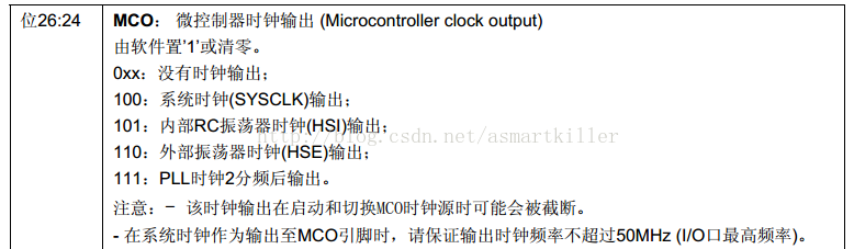
MCO时钟输出 微控制器允许输出时钟信号到外部MCO引脚。相应的GPIO端口寄存器必须被配置为相应功能。
以下四个时钟信号可被选作MCO时钟:
● SYSCLK
● HSI
● HSE
● 除2的PLL时钟
时钟的选择由时钟配置寄存器(RCC_CFGR)中的MCO[2:0]位控制。
下面介绍低速时钟(即是根部3和根部4):
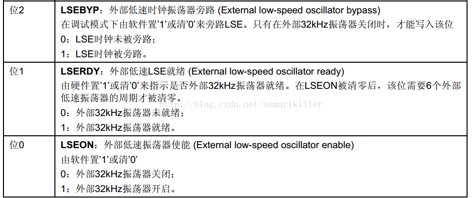
低速外部时钟LSE:LSE晶体是一个32.768kHz的低速外部晶体或陶瓷谐振器。它为实时时钟或者其他定时功能提供一个低功耗且精确的时源。LSE晶体通过在备份域控制寄存器(RCC_BDCR)里的LSEON位启动和关闭。在备份域控制寄存器(RCC_BDCR)里的LSERDY指示LSE晶体振荡是否稳定。在启动阶段,直到这个位被硬件置’1’后,LSE时钟信号才被释放出来。如果在时钟中断寄存器里被允许,可产生中断申请。
外部时钟源(LSE旁路)在这个模式里必须提供一个32.768kHz频率的外部时钟源。你可以通过设置在备份域控制寄存器(RCC_BDCR)里的LSEBYP和LSEON位来选择这个模式。具有50%占空比的外部时钟信号(方波、正弦波或三角波)必须连到OSC32_IN引脚,同时保证OSC32_OUT引脚悬空。
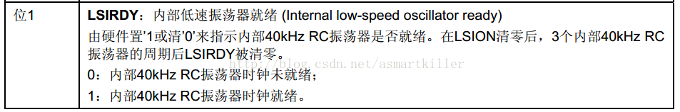
低速内部时钟LSI:LSI RC担当一个低功耗时钟源的角色,它可以在停机和待机模式下保持运行,为独立看门狗和自动唤醒单元提供时钟。 LSI时钟频率大约40kHz(在30kHz和60kHz之间)。进一步信息请参考数据手册中有关电气特性部分。LSI RC可以通过控制/状态寄存器(RCC_CSR)里的LSION位来启动或关闭。在控制/状态寄存器(RCC_CSR)里的LSIRDY位指示低速内部振荡器是否稳定。在启动阶段,直到这个位被硬件设置为’1’后,此时钟才被释放。如果在时钟中断寄存器(RCC_CIR)里被允许,将产生LSI中断申请。注意:
只有大容量和互联型产品可以进行LSI校准。
LSI校准可以通过校准内部低速振荡器LSI来补偿其频率偏移,从而获得精度可接受的RTC时间基数,以及独立看门狗(IWDG)的超时时间(当这些外设以LSI为时钟源)。校准可以通过使用TIM5的输入时钟(TIM5_CLK)测量LSI时钟频率实现。测量以HSE的精度为保证,软件可以通过调整RTC的20位预分频器来获得精确的RTC时钟基数,以及通过计算得到精确的独立看门狗(IWDG)的超时时间。
LSI校准步骤如下:
1. 打开TIM5,设置通道4为输入捕获模式;
2. 设置AFIO_MAPR的TIM5_CH4_IREMAP位为’1’,在内部把LSI连接到TIM5的通道4;
3. 通过TIM5的捕获/比较4事件或者中断来测量LSI时钟频率;
4. 根据测量结果和期望的RTC时间基数和独立看门狗的超时时间,设置20位预分频器。

LSI振荡器将被强制在打开状态,并且不能被关闭。在LSI振荡器稳定后,时钟供应给IWDG。
下面我们来看看小树枝(区域B):
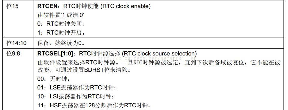
RTC时钟:通过设置备份域控制寄存器(RCC_BDCR)里的RTCSEL[1:0]位,RTCCLK时钟源可以由HSE/128、LSE或LSI时钟提供。除非备份域复位,此选择不能被改变。LSE时钟在备份域里,但HSE和LSI时钟不是。因此:
● 如果LSE被选为RTC时钟:只要VBAT维持供电,尽管VDD供电被切断,RTC仍继续工作。
● 如果LSI被选为自动唤醒单元(AWU)时钟:如果VDD供电被切断,AWU状态不能被保证。。
● 如果HSE时钟128分频后作为RTC时钟:如果VDD供电被切断或内部电压调压器被关闭(1.8V域的供电被切断),则RTC状态不确定。
─
必须设置电源控制寄存器(见4.4.1节)的DPB位(取消后备区域的写保护)为’1’。
关于时钟中断的一些操作,先看看固件中的函数,等后面用到时再仔细看看:
相关寄存器位在时钟中断寄存器(RCC_CIR)中。
RCC库函数中其他一些函数:
一些需要和其他部分有关的函数:等学习到这些章节再说
下一节想学学这些寄存器的地址映像,先开个头
#define RCC ((RCC_TypeDef *) RCC_BASE)
#define RCC_BASE (AHBPERIPH_BASE + 0x1000) #define AHBPERIPH_BASE (PERIPH_BASE + 0x20000)
#define PERIPH_BASE ((uint32_t)0x40000000) /*!< Peripheral base address in the alias region */
由上面的地址可以得出RCC_BASE = ((uint32_t)0x40021000),即将RCC_BASE(地址,为常量)强制转换为指RCC_TypeDef结构体的指针类型的值。即 ((RCC_TypeDef *) ((uint32_t)0x40021000))
“指针类型”是类型,它和int类型一样,也存在"指针类型变量"和"指针类型的值"。“指针类型”“指针类型变量””指针类型的值“经常被简单统称为“指针”。(摘自征服C指针17页)
typedef struct
{
__IO uint32_t CR; //时钟控制寄存器,偏移地址:0x00
__IO uint32_t CFGR; //时钟配置寄存器,偏移地址:0x04
__IO uint32_t CIR; //时钟中断寄存器,偏移地址:0x08
__IO uint32_t APB2RSTR; //APB2外设复位寄存器,偏移地址:0x0C
__IO uint32_t APB1RSTR; //APB1外设复位寄存器,偏移地址:0x10
__IO uint32_t AHBENR; //AHB外设时钟使能寄存器,偏移地址:0x14
__IO uint32_t APB2ENR; //APB2外设时钟使能寄存器,偏移地址:0x18
__IO uint32_t APB1ENR; //APB1外设时钟使能寄存器,偏移地址:0x1C
__IO uint32_t BDCR; //备份域控制寄存器,偏移地址:0x20
__IO uint32_t CSR; //控制/状态寄存器,偏移地址:0x24
#ifdef STM32F10X_CL
__IO uint32_t AHBRSTR;
__IO uint32_t CFGR2;
#endif /* STM32F10X_CL */
#if defined (STM32F10X_LD_VL) || defined (STM32F10X_MD_VL) || defined (STM32F10X_HD_VL)
uint32_t RESERVED0;
__IO uint32_t CFGR2;
#endif /* STM32F10X_LD_VL || STM32F10X_MD_VL || STM32F10X_HD_VL */
} RCC_TypeDef;
通过结构体的存取规则来操作指定地址下的内存(例:RCC->CR)
本文章是基于STM32F103ZE微控制器,主要是详细说明STM32F系列的特性,由于本人是初学者,出现错误是难免的,请大家见谅。固件库采用V3.5.0版本
下面是STM32的时钟树
为使讲解更加清晰,我们把图分解开来,一部分一部分来看:
1、HSI高速内部时钟,RC振荡器,频率为8MHz。
2、HSE高速外部时钟,可接石英/陶瓷谐振器,或接外部时钟源,频率范围为4MHz~16MHz。
3、LSI低速内部时钟,RC振荡器,频率为40kHz。
4、LSE低速外部时钟,接频率为32.768kHz的石英晶体。
如果将时钟系统看作是一颗大树,那么1,2,3,4部分可以看作为树的根部。这里是时钟产生的地方,有关这部分的讲解后面会提到。
下面说的是时钟树的主要躯干部分: 图中的SYSCLK是系统时钟(最大为72MHz),有三种不同的时钟源可以用来驱动系统时钟:HSI振荡器时钟,HSE振荡器时钟,PLL时钟。这三个时钟源由SW确定。(SW是时钟配置寄存器RCC_CFGR中的第1:和0位:系统时钟切换 System clock switch)。系统复位后, HSI振荡器被选为系统时钟。当时钟源被直接或通过PLL间接作为系统时钟时,它将不能被停止。只有当目标时钟源准备就绪了(经过启动稳定阶段的延迟或PLL稳定),从一个时钟源到另一个时钟源的切换才会发生。在被选择时钟源没有就绪时,系统时钟的切换不会发生。直至目标时钟源就绪,才发生切换。在时钟控制寄存器(RCC_CR)里的状态位指示哪个时钟已经准备好了,哪个时钟目前被用作系统时钟。I2S音频总线时钟直接来源于系统时钟。
/**
* @brief  Configures the system clock (SYSCLK).
配置系统时钟
* @param  RCC_SYSCLKSource: specifies the clock source used as system clock.
指定时钟源作为系统时钟
*   This parameter can be one of the following values:
*     @arg RCC_SYSCLKSource_HSI: HSI selected as system clock HSI选为系统时钟
#define RCC_SYSCLKSource_HSI ((uint32_t)0x00000000)
*     @arg RCC_SYSCLKSource_HSE: HSE selected as system clock HSE选为系统时钟
#define RCC_SYSCLKSource_HSE ((uint32_t)0x00000001)
*     @arg RCC_SYSCLKSource_PLLCLK: PLL selected as system clock PLL选为系统时钟
#define RCC_SYSCLKSource_PLLCLK ((uint32_t)0x00000002)
* @retval None
*/
void RCC_SYSCLKConfig(uint32_t RCC_SYSCLKSource)
{
uint32_t tmpreg = 0;
/* Check the parameters */
assert_param(IS_RCC_SYSCLK_SOURCE(RCC_SYSCLKSource));
tmpreg = RCC->CFGR;
/* Clear SW[1:0] bits 清除系统时钟切换位*/
tmpreg &= CFGR_SW_Mask;
/* Set SW[1:0] bits according to RCC_SYSCLKSource value */
tmpreg |= RCC_SYSCLKSource;
/* Store the new value 设置新状态*/
RCC->CFGR = tmpreg;
}
/**
* @brief Returns the clo
1b4e8
ck source used as system clock.
返回系统时钟选用的时钟源
* @param None
* @retval The clock source used as system clock. The returned value can
* be one of the following:
* - 0x00: HSI used as system clock HSI作为系统时钟
* - 0x04: HSE used as system clock HSE作为系统时钟
* - 0x08: PLL used as system clock PLL作为系统时钟
*/
uint8_t RCC_GetSYSCLKSource(void)
{
return ((uint8_t)(RCC->CFGR & CFGR_SWS_Mask));
} 现在我们再从根部详细说起:高速外部时钟信号HSE由两种时钟源产生,即HSE用户外部时钟(HSE旁路)和HSE外部晶体/陶瓷谐振器。
1.第一种模式:外部时钟源,它的频率最高可达25MHz。用户可以通过设置在时钟控制寄存器中的HSEBYP和HSEON位来选择这一模式。外部时钟信号(50%占空比的方波、正弦波或三角波)必须连接到SOC_IN引脚,同时保证OSC_OUT悬空。
2.第二种模式为外部晶体/陶瓷谐振器。在这种情况下需要等晶体振荡器稳定才能采用。
下面该图为这两种方式的硬件接法:这两种模式通过硬件配置和外部高速时钟旁路位来配置。
在时钟控制寄存器RCC_CR中的HSERDY位用来指示高速外部振荡器是否稳定。在启动时,直到这一位被硬件置’1’,时钟才被释放出来。如果在时钟中断寄存器RCC_CIR中允许产生中断,将会产生相应中断。HSE晶体可以通过设置时钟控制寄存器里RCC_CR中的HSEON位被启动和关闭。
/**
* @brief  Configures the External High Speed oscillator (HSE).
配置外部高速振荡器
* @note   HSE can not be stopped if it is used directly or through the PLL as system clock.
HSE不能被停止如果它已经作为系统时钟在使用或者通过PLL作为时钟在使用
* @param  RCC_HSE: specifies the new state of the HSE.  指明HSE的新状态
*   This parameter can be one of the following values:  参数
*     @arg RCC_HSE_OFF: HSE oscillator OFF   //#define RCC_HSE_OFF((uint32_t)0x00000000)   HSE晶体振荡器关
*     @arg RCC_HSE_ON: HSE oscillator ON     //#define RCC_HSE_ON ((uint32_t)0x00010000)   HSE晶体振荡器开
*     @arg RCC_HSE_Bypass: HSE oscillator bypassed with external clock HSE                 HSE旁路模式
//#define RCC_HSE_Bypass ((uint32_t)0x00040000)
* @retval None
*/
void RCC_HSEConfig(uint32_t RCC_HSE)
{
/* Check the parameters 检查参数*/
assert_param(IS_RCC_HSE(RCC_HSE));
//#define IS_RCC_HSE(HSE) (((HSE) == RCC_HSE_OFF) || ((HSE) == RCC_HSE_ON) || \
((HSE) == RCC_HSE_Bypass))    //反斜杠起到换行作用,用于宏定义和字符串换行。其中宏定义中使用居多。

/* Reset HSEON and HSEBYP bits before configuring the HSE 复位HSE使能和HSE旁路------------------*/
/* Reset HSEON bit */
RCC->CR &= CR_HSEON_Reset;
/* Reset HSEBYP bit */
RCC->CR &= CR_HSEBYP_Reset;
/* Configure HSE (RCC_HSE_OFF is already covered by the code section above) 复位HSE在上述复位过程中已经包含 */
switch(RCC_HSE)
{
case RCC_HSE_ON:
/* Set HSEON bit 使能HSE*/
RCC->CR |= CR_HSEON_Set;
break;

case RCC_HSE_Bypass:
/* Set HSEBYP and HSEON bits 使能HSE旁路和HSE时钟*/
RCC->CR |= CR_HSEBYP_Set | CR_HSEON_Set;
break;

default:
break;
}
}
/**
* @brief Waits for HSE start-up.
等待直到外部高速晶振稳定
* @param None
* @retval An ErrorStatus enumuration value: 错误状态祥表
* - SUCCESS: HSE oscillator is stable and ready to use
* - ERROR: HSE oscillator not yet ready
typedef enum {ERROR = 0, SUCCESS = !ERROR} ErrorStatus; ErrorStatus是枚举类型
typedef enum {RESET = 0, SET = !RESET} FlagStatus, ITStatus; FlagStatus是枚举类型
*/
ErrorStatus RCC_WaitForHSEStartUp(void)
{
__IO uint32_t StartUpCounter = 0;
ErrorStatus status = ERROR;
FlagStatus HSEStatus = RESET;
/* Wait till HSE is ready and if Time out is reached exit 直到HSE稳定或者起振阀值时间到了才退出*/
do
{
HSEStatus = RCC_GetFlagStatus(RCC_FLAG_HSERDY);
StartUpCounter++;
} while((StartUpCounter != HSE_STARTUP_TIMEOUT) && (HSEStatus == RESET));
//#define HSE_STARTUP_TIMEOUT ((uint16_t)0x0500) /*!< Time out for HSE start up */
if (RCC_GetFlagStatus(RCC_FLAG_HSERDY) != RESET)
{
status = SUCCESS; //HSE稳定
}
else
{
status = ERROR; //HSE未能起振
}
return (status);
}高速外部时钟信号HSE可直接作为SYSCLK系统时钟(通过SW选择),也可以经过PLLXTPRE多路复用器选择直接或者二分频后输给PLLMUL倍频器后(RCC_PLLConfig函数中配置)作为系统时钟。
这里还有监控SYSCLK时钟的特性,该特性跟HSE振荡器有关:
时钟安全系统(CSS):时钟安全系统可以通过软件被激活。一旦其被激活,时钟监测器将在HSE振荡器启动延迟后被使能,并在HSE时钟关闭后关闭。如果HSE时钟发生故障,HSE振荡器被自动关闭,时钟失效事件将被送到高级定时器(TIM1和TIM8)的刹车输入端,并产生时钟安全中断CSSI,允许软件完成营救操作。此CSSI中断连接到Cortex™-M3的NMI中断(不可屏蔽中断)。注意:
一旦CSS被激活,并且HSE时钟出现故障, CSS中断就产生,并且NMI也自动产生。 NMI将被不断执行,直到CSS中断挂起位被清除。因此,在NMI的处理程序中必须通过设置时钟中断寄存器(RCC_CIR)里的CSSC位来清除CSS中断。如果HSE振荡器被直接或间接地作为系统时钟,(间接的意思是:它被作为PLL输入时钟,并且PLL时钟被作为系统时钟),时钟故障将导致系统时钟自动切换到HSI振荡器,同时外部HSE振荡器被关闭。在时钟失效时,如果HSE振荡器时钟(被分频或未被分频)是用作系统时钟的PLL的输入时钟,PLL也将被关闭。
/**
* @brief  Enables or disables the Clock Security System.
使能或者失能CSS
* @param  NewState: new state of the Clock Security System..
*   This parameter can be: ENABLE or DISABLE.
* @retval None
*/
void RCC_ClockSecuritySystemCmd(FunctionalState NewState)
{
/* Check the parameters */
assert_param(IS_FUNCTIONAL_STATE(NewState));
*(__IO uint32_t *) CR_CSSON_BB = (uint32_t)NewState;
}高速内部时钟信号HSI由内部8MHz的RC振荡器产生,可直接作为系统时钟或在2分频后作为PLL输入。当HSI被用于作为PLL时钟的输入时,系统时钟能得到的最大频率是64MHz。HSI RC振荡器能够在不需要任何外部器件的条件下提供系统时钟。它的启动时间比HSE晶体振荡器短。然而,即使在校准之后它的时钟频率精度仍较差。校准制造工艺决定了不同芯片的RC振荡器频率会不同,这就是为什么每个芯片的HSI时钟频率在出厂前已经被ST校准到1%(25°C)的原因。系统复位时,工厂校准值被装载到时钟控制寄存器的HSICAL[7:0]位。如果用户的应用基于不同的电压或环境温度,这将会影响RC振荡器的精度。可以通过时钟控制寄存器里的HSITRIM[4:0]位来调整HSI频率。时钟控制寄存器中的HSIRDY位用来指示HSI
RC振荡器是否稳定。在时钟启动过程中,直到这一位被硬件置’1’, HSI RC输出时钟才被释放。 HSI RC可由时钟控制寄存器中的HSION位来启动和关闭。如果HSE晶体振荡器失效, HSI时钟会被作为备用时钟源。
/**
* @brief  Adjusts the Internal High Speed oscillator (HSI) calibration value.
调整HSI精度值
* @param  HSICalibrationValue: specifies the calibration trimming value.
*   This parameter must be a number between 0 and 0x1F.
* @retval None
*/
void RCC_AdjustHSICalibrationValue(uint8_t HSICalibrationValue)
{
uint32_t tmpreg = 0;
/* Check the parameters */
assert_param(IS_RCC_CALIBRATION_VALUE(HSICalibrationValue));
tmpreg = RCC->CR;
/* Clear HSITRIM[4:0] bits */
tmpreg &= CR_HSITRIM_Mask;
/* Set the HSITRIM[4:0] bits according to HSICalibrationValue value */
tmpreg |= (uint32_t)HSICalibrationValue << 3;
/* Store the new value */
RCC->CR = tmpreg;
}
/**
* @brief Enables or disables the Internal High Speed oscillator (HSI).
使能或失能内部高速晶振
* @note HSI can not be stopped if it is used directly or through the PLL as system clock.
HSI不能被停止如果HSI直接作为系统时钟或通过PLL间接作为系统时钟
* @param NewState: new state of the HSI. This parameter can be: ENABLE or DISABLE.
* @retval None
*/
void RCC_HSICmd(FunctionalState NewState)
{
/* Check the parameters */
assert_param(IS_FUNCTIONAL_STATE(NewState));
//typedef enum {DISABLE = 0, ENABLE = !DISABLE} FunctionalState;
//#define IS_FUNCTIONAL_STATE(STATE) (((STATE) == DISABLE) || ((STATE) == ENABLE))
*(__IO uint32_t *) CR_HSION_BB = (uint32_t)NewState;
/* Alias word address of HSION bit */
//#define PERIPH_BB_BASE ((uint32_t)0x42000000) /*!< Peripheral base address in the bit-band region */
//#define CR_OFFSET (RCC_OFFSET + 0x00) #define HSION_BitNumber 0x00
//#define CR_HSION_BB (PERIPH_BB_BASE + (CR_OFFSET * 32) + (HSION_BitNumber * 4))
}下面来看看时钟树躯干部分(即标号5处)的相关内容:
5.PLL可以用来倍频HSI RC的输出时钟或HSE晶体输出时钟。PLL的设置(选择HIS振荡器除2或HSE振荡器为PLL的输入时钟,和选择倍频因子)必须在其被激活前完成。一旦PLL被激活,这些参数就不能被改动。如果PLL中断在时钟中断寄存器里被允许,当PLL准备就绪时,可产生中断申请。
/**
* @brief  Configures the PLL clock source and multiplication factor.
设置PLL时钟源及倍频系数
* @note   This function must be used only when the PLL is disabled.
当PLL使能时才能使用
* @param  RCC_PLLSource: specifies the PLL entry clock source.   指定输入PLL的时钟源
*   For @b STM32_Connectivity_line_devices or @b STM32_Value_line_devices,
*   this parameter can be one of the following values:
*     @arg RCC_PLLSource_HSI_Div2: HSI oscillator clock divided by 2 selected as PLL clock entry
*     @arg RCC_PLLSource_PREDIV1: PREDIV1 clock selected as PLL clock entry
*   For @b other_STM32_devices, this parameter can be one of the following values:
*     @arg RCC_PLLSource_HSI_Div2: HSI oscillator clock divided by 2 selected as PLL clock entry
#define RCC_PLLSource_HSI_Div2 ((uint32_t)0x00000000)
*     @arg RCC_PLLSource_HSE_Div1: HSE oscillator clock selected as PLL clock entry
#define RCC_PLLSource_HSE_Div1 ((uint32_t)0x00010000)
*     @arg RCC_PLLSource_HSE_Div2: HSE oscillator clock divided by 2 selected as PLL clock entry
#define RCC_PLLSource_HSE_Div2 ((uint32_t)0x00030000)
* @param  RCC_PLLMul: specifies the PLL multiplication factor.
*   For @b STM32_Connectivity_line_devices, this parameter can be RCC_PLLMul_x where x:{[4,9], 6_5}
*   For @b other_STM32_devices, this parameter can be RCC_PLLMul_x where x:[2,16]
* @retval None
*/
void RCC_PLLConfig(uint32_t RCC_PLLSource, uint32_t RCC_PLLMul)
{
uint32_t tmpreg = 0;

/* Check the parameters */
assert_param(IS_RCC_PLL_SOURCE(RCC_PLLSource));
assert_param(IS_RCC_PLL_MUL(RCC_PLLMul));

tmpreg = RCC->CFGR;
/* Clear PLLSRC, PLLXTPRE and PLLMUL[3:0] bits */
//清除PLL输入时钟源,HSE分频器作为PLL输入位,PLL倍频系数位
tmpreg &= CFGR_PLL_Mask;
/* Set the PLL configuration bits 设置PLL配置位*/
tmpreg |= RCC_PLLSource | RCC_PLLMul;
/* Store the new value 配置*/
RCC->CFGR = tmpreg;
}
/**
* @brief Enables or disables the PLL.
使能或者使能PLL
* @note The PLL can not be disabled if it is used as system clock.
* @param NewState: new state of the PLL. This parameter can be: ENABLE or DISABLE.
* @retval None
*/
void RCC_PLLCmd(FunctionalState NewState)
{
/* Check the parameters */
assert_param(IS_FUNCTIONAL_STATE(NewState));
*(__IO uint32_t *) CR_PLLON_BB = (uint32_t)NewState;
}接下来可以介绍一下时钟树的树叶部分了:
PLL时钟的一个小流向(即是图中所标C区域):如果需要在应用中使用USB接口, PLL必须被设置为输出48或72MHZ时钟,用于提供48MHz的USBCLK时钟。
USB时钟来源于PLLCLK,通过USB分频器为USB外设提供48MHZ时钟。由于USB时钟分频器只能1分频和1.5分频,所以PLL出来的时钟频率只能是48MHz和72MHz。
/**
* @brief  Configures the USB clock (USBCLK).
配置USB时钟
* @param  RCC_USBCLKSource: specifies the USB clock source. This clock is
*   derived from the PLL output.
*   This parameter can be one of the following values:
*     @arg RCC_USBCLKSource_PLLCLK_1Div5: PLL clock divided by 1,5 selected as USB
*                                     clock source ((uint8_t)0x00)
*     @arg RCC_USBCLKSource_PLLCLK_Div1: PLL clock selected as USB clock source ((uint8_t)0x01)
USB时钟来源于PLL时钟,可以对PLL进行1.5或1分频作为USB时钟输出(48MHZ)
* @retval None
*/
void RCC_USBCLKConfig(uint32_t RCC_USBCLKSource)
{
/* Check the parameters */
assert_param(IS_RCC_USBCLK_SOURCE(RCC_USBCLKSource));

*(__IO uint32_t *) CFGR_USBPRE_BB = RCC_USBCLKSource;
}
下面是大树枝叶最为茂密的地方了:
上面是以哪些时钟源可以作为SYSCLK时钟源展开的,下面说明由SYSCLK得到AHB时钟(HCLK),低速APB1时钟,高速APB2时钟。AHB和APB2域的最大频率是72MHz。 APB1域的最大允许频率是36MHz。
配置AHB时钟的频率即分频系数。这是时钟数由SYSCLK到AHB的第一个节点(即图中D标号下方的AHB预分频器模块)。
/**
* @brief  Configures the AHB clock (HCLK).
配置AHB时钟(HCLK)
* @param  RCC_SYSCLK: defines the AHB clock divider. This clock is derived from
*   the system clock (SYSCLK).
*   This parameter can be one of the following values:
*     @arg RCC_SYSCLK_Div1: AHB clock = SYSCLK         ((uint32_t)0x00000000)
*     @arg RCC_SYSCLK_Div2: AHB clock = SYSCLK/2       ((uint32_t)0x00000080)
*     @arg RCC_SYSCLK_Div4: AHB clock = SYSCLK/4       ((uint32_t)0x00000090)
*     @arg RCC_SYSCLK_Div8: AHB clock = SYSCLK/8       ((uint32_t)0x000000A0)
*     @arg RCC_SYSCLK_Div16: AHB clock = SYSCLK/16     ((uint32_t)0x000000B0)
*     @arg RCC_SYSCLK_Div64: AHB clock = SYSCLK/64     ((uint32_t)0x000000C0)
*     @arg RCC_SYSCLK_Div128: AHB clock = SYSCLK/128   ((uint32_t)0x000000D0)
*     @arg RCC_SYSCLK_Div256: AHB clock = SYSCLK/256   ((uint32_t)0x000000E0)
*     @arg RCC_SYSCLK_Div512: AHB clock = SYSCLK/512   ((uint32_t)0x000000F0)
* @retval None
*/
void RCC_HCLKConfig(uint32_t RCC_SYSCLK)
{
uint32_t tmpreg = 0;
/* Check the parameters */
assert_param(IS_RCC_HCLK(RCC_SYSCLK));
tmpreg = RCC->CFGR;
/* Clear HPRE[3:0] bits */
tmpreg &= CFGR_HPRE_Reset_Mask;
/* Set HPRE[3:0] bits according to RCC_SYSCLK value */
tmpreg |= RCC_SYSCLK;
/* Store the new value */
RCC->CFGR = tmpreg;
}AHB时钟下挂载了外设(如DMA,SRAM,FLITF,CRC,FSMC,SDIO)和APB1分频器和APB2分频器。RCC通过AHB时钟(HCLK)8分频后作为Cortex系统定时器(SysTick)的外部时钟。通过对SysTick控制与状态寄存器的设置,可选择上述时钟或Cortex(HCLK)时钟作为SysTick时钟。FCLK是Cortex™-M3的自由运行时钟。/**
* @brief Enables or disables the AHB peripheral clock.
使能或者失能AHB外设时钟
* @param RCC_AHBPeriph: specifies the AHB peripheral to gates its clock.
*
* For @b STM32_Connectivity_line_devices, this parameter can be any combination
* of the following values:
* @arg RCC_AHBPeriph_DMA1
* @arg RCC_AHBPeriph_DMA2
* @arg RCC_AHBPeriph_SRAM
* @arg RCC_AHBPeriph_FLITF
* @arg RCC_AHBPeriph_CRC
* @arg RCC_AHBPeriph_OTG_FS
* @arg RCC_AHBPeriph_ETH_MAC
* @arg RCC_AHBPeriph_ETH_MAC_Tx
* @arg RCC_AHBPeriph_ETH_MAC_Rx
*
* For @b other_STM32_devices, this parameter can be any combination of the
* following values:
* @arg RCC_AHBPeriph_DMA1 ((uint32_t)0x00000001)
* @arg RCC_AHBPeriph_DMA2 ((uint32_t)0x00000002)
* @arg RCC_AHBPeriph_SRAM ((uint32_t)0x00000004)
* @arg RCC_AHBPeriph_FLITF ((uint32_t)0x00000010)
* @arg RCC_AHBPeriph_CRC ((uint32_t)0x00000040)
* @arg RCC_AHBPeriph_FSMC ((uint32_t)0x00000100)
* @arg RCC_AHBPeriph_SDIO ((uint32_t)0x00000400)
*
* @note SRAM and FLITF clock can be disabled only during sleep mode.
SRAM和FLITF时钟只能在睡眠模式下被失能
* @param NewState: new state of the specified peripheral clock.
* This parameter can be: ENABLE or DISABLE.
* @retval None
*/
void RCC_AHBPeriphClockCmd(uint32_t RCC_AHBPeriph, FunctionalState NewState)
{
/* Check the parameters */
assert_param(IS_RCC_AHB_PERIPH(RCC_AHBPeriph));
assert_param(IS_FUNCTIONAL_STATE(NewState));
if (NewState != DISABLE)
{
RCC->AHBENR |= RCC_AHBPeriph;
//AHBENR为AHB外设时钟使能寄存器
}
else
{
RCC->AHBENR &= ~RCC_AHBPeriph;
}
}APB1分频器,配置APB1分频器系数,从而获得低速APB1时钟(PCLK1),最大不超过36MHZ。
/**
* @brief  Configures the Low Speed APB clock (PCLK1).
配置低速APB时钟
* @param  RCC_HCLK: defines the APB1 clock divider. This clock is derived from
*   the AHB clock (HCLK).
*   This parameter can be one of the following values:
*     @arg RCC_HCLK_Div1: APB1 clock = HCLK
*     @arg RCC_HCLK_Div2: APB1 clock = HCLK/2
*     @arg RCC_HCLK_Div4: APB1 clock = HCLK/4
*     @arg RCC_HCLK_Div8: APB1 clock = HCLK/8
*     @arg RCC_HCLK_Div16: APB1 clock = HCLK/16
* @retval None
*/
void RCC_PCLK1Config(uint32_t RCC_HCLK)
{
uint32_t tmpreg = 0;
/* Check the parameters */
assert_param(IS_RCC_PCLK(RCC_HCLK));
tmpreg = RCC->CFGR;
/* Clear PPRE1[2:0] bits */
tmpreg &= CFGR_PPRE1_Reset_Mask;
/* Set PPRE1[2:0] bits according to RCC_HCLK value */
tmpreg |= RCC_HCLK;
/* Store the new value */
RCC->CFGR = tmpreg;
}
APB1分频器下挂载的外设(如TIM2,TIM3,TIM4,TIM5, TIM6, TIM7,WWDG,SPI2, SPI3,USART2, USART3, USART4, USART5, I2C1, I2C2,USB, CAN1, BKP,PWR, DAC, )
/**
* @brief  Enables or disables the Low Speed APB (APB1) peripheral clock.
使能或者失能APB1外设时钟
* @param  RCC_APB1Periph: specifies the APB1 peripheral to gates its clock.
*   This parameter can be any combination of the following values:
*     @arg RCC_APB1Periph_TIM2, RCC_APB1Periph_TIM3, RCC_APB1Periph_TIM4,
*          RCC_APB1Periph_TIM5, RCC_APB1Periph_TIM6, RCC_APB1Periph_TIM7,
*          RCC_APB1Periph_WWDG, RCC_APB1Periph_SPI2, RCC_APB1Periph_SPI3,
*          RCC_APB1Periph_USART2, RCC_APB1Periph_USART3, RCC_APB1Periph_USART4,
*          RCC_APB1Periph_USART5, RCC_APB1Periph_I2C1, RCC_APB1Periph_I2C2,
*          RCC_APB1Periph_USB, RCC_APB1Periph_CAN1, RCC_APB1Periph_BKP,
*          RCC_APB1Periph_PWR, RCC_APB1Periph_DAC,

RCC_APB1Periph_CEC,
*          RCC_APB1Periph_TIM12, RCC_APB1Periph_TIM13, RCC_APB1Periph_TIM14
* @param  NewState: new state of the specified peripheral clock.
*   This parameter can be: ENABLE or DISABLE.
* @retval None
*/
void RCC_APB1PeriphClockCmd(uint32_t RCC_APB1Periph, FunctionalState NewState)
{
/* Check the parameters */
assert_param(IS_RCC_APB1_PERIPH(RCC_APB1Periph));
assert_param(IS_FUNCTIONAL_STATE(NewState));
if (NewState != DISABLE)
{
RCC->APB1ENR |= RCC_APB1Periph;
}
else
{
RCC->APB1ENR &= ~RCC_APB1Periph;
}
}
/**
* @brief Forces or releases Low Speed APB (APB1) peripheral reset.
强制复位或置位APB1外设
* @param RCC_APB1Periph: specifies the APB1 peripheral to reset.
* This parameter can be any combination of the following values:
* @arg RCC_APB1Periph_TIM2, RCC_APB1Periph_TIM3, RCC_APB1Periph_TIM4,
* RCC_APB1Periph_TIM5, RCC_APB1Periph_TIM6, RCC_APB1Periph_TIM7,
* RCC_APB1Periph_WWDG, RCC_APB1Periph_SPI2, RCC_APB1Periph_SPI3,
* RCC_APB1Periph_USART2, RCC_APB1Periph_USART3, RCC_APB1Periph_USART4,
* RCC_APB1Periph_USART5, RCC_APB1Periph_I2C1, RCC_APB1Periph_I2C2,
* RCC_APB1Periph_USB, RCC_APB1Periph_CAN1, RCC_APB1Periph_BKP,
* RCC_APB1Periph_PWR, RCC_APB1Periph_DAC, RCC_APB1Periph_CEC,
* RCC_APB1Periph_TIM12, RCC_APB1Periph_TIM13, RCC_APB1Periph_TIM14
* @param NewState: new state of the specified peripheral clock.
* This parameter can be: ENABLE or DISABLE.
* @retval None
*/
void RCC_APB1PeriphResetCmd(uint32_t RCC_APB1Periph, FunctionalState NewState)
{
/* Check the parameters */
assert_param(IS_RCC_APB1_PERIPH(RCC_APB1Periph));
assert_param(IS_FUNCTIONAL_STATE(NewState));
if (NewState != DISABLE)
{
RCC->APB1RSTR |= RCC_APB1Periph;
//APB1RSTR为APB1外设复位寄存器
}
else
{
RCC->APB1RSTR &= ~RCC_APB1Periph;
}
}APB2分频器,配置APB2分频器系数,从而获得高速APB2时钟(PCLK2),最大不超过72MHZ。
/**
* @brief  Configures the High Speed APB clock (PCLK2).
配置高速时钟APB(PCLK2)
* @param  RCC_HCLK: defines the APB2 clock divider. This clock is derived from
*   the AHB clock (HCLK).
*   This parameter can be one of the following values:
*     @arg RCC_HCLK_Div1: APB2 clock = HCLK
*     @arg RCC_HCLK_Div2: APB2 clock = HCLK/2
*     @arg RCC_HCLK_Div4: APB2 clock = HCLK/4
*     @arg RCC_HCLK_Div8: APB2 clock = HCLK/8
*     @arg RCC_HCLK_Div16: APB2 clock = HCLK/16
* @retval None
*/
void RCC_PCLK2Config(uint32_t RCC_HCLK)
{
uint32_t tmpreg = 0;
/* Check the parameters */
assert_param(IS_RCC_PCLK(RCC_HCLK));
tmpreg = RCC->CFGR;
/* Clear PPRE2[2:0] bits */
tmpreg &= CFGR_PPRE2_Reset_Mask;
/* Set PPRE2[2:0] bits according to RCC_HCLK value */
tmpreg |= RCC_HCLK << 3;
/* Store the new value */
RCC->CFGR = tmpreg;
}APB2分频器下挂载的外设/**
* @brief Enables or disables the High Speed APB (APB2) peripheral clock.
使能或者失能APB2外设时钟
* @param RCC_APB2Periph: specifies the APB2 peripheral to gates its clock.
* This parameter can be any combination of the following values:
* @arg RCC_APB2Periph_AFIO, RCC_APB2Periph_GPIOA, RCC_APB2Periph_GPIOB,
* RCC_APB2Periph_GPIOC, RCC_APB2Periph_GPIOD, RCC_APB2Periph_GPIOE,
* RCC_APB2Periph_GPIOF, RCC_APB2Periph_GPIOG, RCC_APB2Periph_ADC1,
* RCC_APB2Periph_ADC2, RCC_APB2Periph_TIM1, RCC_APB2Periph_SPI1,
* RCC_APB2Periph_TIM8, RCC_APB2Periph_USART1, RCC_APB2Periph_ADC3,
* RCC_APB2Periph_TIM15, RCC_APB2Periph_TIM16, RCC_APB2Periph_TIM17,
* RCC_APB2Periph_TIM9, RCC_APB2Periph_TIM10, RCC_APB2Periph_TIM11
* @param NewState: new state of the specified peripheral clock.
* This parameter can be: ENABLE or DISABLE.
* @retval None
*/
void RCC_APB2PeriphClockCmd(uint32_t RCC_APB2Periph, FunctionalState NewState)
{
/* Check the parameters */
assert_param(IS_RCC_APB2_PERIPH(RCC_APB2Periph));
assert_param(IS_FUNCTIONAL_STATE(NewState));
if (NewState != DISABLE)
{
RCC->APB2ENR |= RCC_APB2Periph;
//APB2ENR为APB2外设时钟使能寄存器
}
else
{
RCC->APB2ENR &= ~RCC_APB2Periph;
}
}/**
* @brief Forces or releases High Speed APB (APB2) peripheral reset.
强制复位或置位APB2外设
* @param RCC_APB2Periph: specifies the APB2 peripheral to reset.
* This parameter can be any combination of the following values:
* @arg RCC_APB2Periph_AFIO, RCC_APB2Periph_GPIOA, RCC_APB2Periph_GPIOB,
* RCC_APB2Periph_GPIOC, RCC_APB2Periph_GPIOD, RCC_APB2Periph_GPIOE,
* RCC_APB2Periph_GPIOF, RCC_APB2Periph_GPIOG, RCC_APB2Periph_ADC1,
* RCC_APB2Periph_ADC2, RCC_APB2Periph_TIM1, RCC_APB2Periph_SPI1,
* RCC_APB2Periph_TIM8, RCC_APB2Periph_USART1, RCC_APB2Periph_ADC3,
* RCC_APB2Periph_TIM15, RCC_APB2Periph_TIM16, RCC_APB2Periph_TIM17,
* RCC_APB2Periph_TIM9, RCC_APB2Periph_TIM10, RCC_APB2Periph_TIM11
* @param NewState: new state of the specified peripheral reset.
* This parameter can be: ENABLE or DISABLE.
* @retval None
*/
void RCC_APB2PeriphResetCmd(uint32_t RCC_APB2Periph, FunctionalState NewState)
{
/* Check the parameters */
assert_param(IS_RCC_APB2_PERIPH(RCC_APB2Periph));
assert_param(IS_FUNCTIONAL_STATE(NewState));
if (NewState != DISABLE)
{
RCC->APB2RSTR |= RCC_APB2Periph;
//APB2RSTR为APB2外设复位寄存器
}
else
{
RCC->APB2RSTR &= ~RCC_APB2Periph;
}
}ADC时钟由高速APB2时钟经2、 4、 6或8分频后获得。/**
* @brief Configures the ADC clock (ADCCLK)
配置ADC时钟
* @param RCC_PCLK2: defines the ADC clock divider. This clock is derived from
* the APB2 clock (PCLK2). ADC时钟来源于高速APB2时钟
* This parameter can be one of the following values:
* @arg RCC_PCLK2_Div2: ADC clock = PCLK2/2 ((uint32_t)0x00000000)
* @arg RCC_PCLK2_Div4: ADC clock = PCLK2/4 ((uint32_t)0x00004000)
* @arg RCC_PCLK2_Div6: ADC clock = PCLK2/6 ((uint32_t)0x00008000)
* @arg RCC_PCLK2_Div8: ADC clock = PCLK2/8 ((uint32_t)0x0000C000)
* @retval None
*/
void RCC_ADCCLKConfig(uint32_t RCC_PCLK2)
{
uint32_t tmpreg = 0;
/* Check the parameters */
assert_param(IS_RCC_ADCCLK(RCC_PCLK2));
tmpreg = RCC->CFGR;
/* Clear ADCPRE[1:0] bits 清除ADC预分频位*/
tmpreg &= CFGR_ADCPRE_Reset_Mask;
/* Set ADCPRE[1:0] bits according to RCC_PCLK2 value */
tmpreg |= RCC_PCLK2;
/* Store the new value 配置*/
RCC->CFGR = tmpreg;
}NOTE:定时器时钟频率分配由硬件按以下2种情况自动设置:
1. 如果相应的APB预分频系数是1,定时器的时钟频率与所在APB总线频率一致。
2. 否则,定时器的时钟频率被设为与其相连的APB总线频率的2倍。
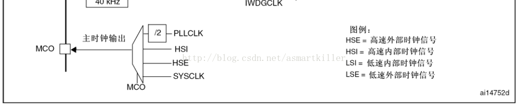
这里我们来看一个比较特别的一根小树枝:
MCO时钟输出 微控制器允许输出时钟信号到外部MCO引脚。相应的GPIO端口寄存器必须被配置为相应功能。
以下四个时钟信号可被选作MCO时钟:
● SYSCLK
● HSI
● HSE
● 除2的PLL时钟
时钟的选择由时钟配置寄存器(RCC_CFGR)中的MCO[2:0]位控制。
/**
* @brief  Selects the clock source to output on MCO pin.
选择输出到MCO引脚的时钟源
* @param  RCC_MCO: specifies the clock source to output.
*
*   For @b STM32_Connectivity_line_devices, this parameter can be one of the
*   following values:
*     @arg RCC_MCO_NoClock: No clock selected
*     @arg RCC_MCO_SYSCLK: System clock selected
*     @arg RCC_MCO_HSI: HSI oscillator clock selected
*     @arg RCC_MCO_HSE: HSE oscillator clock selected
*     @arg RCC_MCO_PLLCLK_Div2: PLL clock divided by 2 selected
*     @arg RCC_MCO_PLL2CLK: PLL2 clock selected
*     @arg RCC_MCO_PLL3CLK_Div2: PLL3 clock divided by 2 selected
*     @arg RCC_MCO_XT1: External 3-25 MHz oscillator clock selected
*     @arg RCC_MCO_PLL3CLK: PLL3 clock selected
*
*   For  @b other_STM32_devices, this parameter can be one of the following values:
*     @arg RCC_MCO_NoClock: No clock selected
*     @arg RCC_MCO_SYSCLK: System clock selected
*     @arg RCC_MCO_HSI: HSI oscillator clock selected
*     @arg RCC_MCO_HSE: HSE oscillator clock selected
*     @arg RCC_MCO_PLLCLK_Div2: PLL clock divided by 2 selected
*
* @retval None
*/
void RCC_MCOConfig(uint8_t RCC_MCO)
{
/* Check the parameters */
assert_param(IS_RCC_MCO(RCC_MCO));

/* Perform Byte access to MCO bits to select the MCO source */
*(__IO uint8_t *) CFGR_BYTE4_ADDRESS = RCC_MCO;
}
下面介绍低速时钟(即是根部3和根部4):
低速外部时钟LSE:LSE晶体是一个32.768kHz的低速外部晶体或陶瓷谐振器。它为实时时钟或者其他定时功能提供一个低功耗且精确的时源。LSE晶体通过在备份域控制寄存器(RCC_BDCR)里的LSEON位启动和关闭。在备份域控制寄存器(RCC_BDCR)里的LSERDY指示LSE晶体振荡是否稳定。在启动阶段,直到这个位被硬件置’1’后,LSE时钟信号才被释放出来。如果在时钟中断寄存器里被允许,可产生中断申请。
外部时钟源(LSE旁路)在这个模式里必须提供一个32.768kHz频率的外部时钟源。你可以通过设置在备份域控制寄存器(RCC_BDCR)里的LSEBYP和LSEON位来选择这个模式。具有50%占空比的外部时钟信号(方波、正弦波或三角波)必须连到OSC32_IN引脚,同时保证OSC32_OUT引脚悬空。
/**
* @brief  Configures the External Low Speed oscillator (LSE).
配置外部低速晶振
* @param  RCC_LSE: specifies the new state of the LSE.
*   This parameter can be one of the following values:
*     @arg RCC_LSE_OFF: LSE oscillator OFF
*     @arg RCC_LSE_ON: LSE oscillator ON
*     @arg RCC_LSE_Bypass: LSE oscillator bypassed with external clock
* @retval None
*/
void RCC_LSEConfig(uint8_t RCC_LSE)
{
/* Check the parameters */
assert_param(IS_RCC_LSE(RCC_LSE));
/* Reset LSEON and LSEBYP bits before configuring the LSE ------------------*/
/* Reset LSEON bit 复位外部低速振荡器使能位*/
*(__IO uint8_t *) BDCR_ADDRESS = RCC_LSE_OFF;
/* Reset LSEBYP bit 复位外部低速时钟振荡器旁路*/
*(__IO uint8_t *) BDCR_ADDRESS = RCC_LSE_OFF;
/* Configure LSE (RCC_LSE_OFF is already covered by the code section above) */
switch(RCC_LSE)
{
case RCC_LSE_ON:
/* Set LSEON bit */
*(__IO uint8_t *) BDCR_ADDRESS = RCC_LSE_ON;
break;

case RCC_LSE_Bypass:
/* Set LSEBYP and LSEON bits */
*(__IO uint8_t *) BDCR_ADDRESS = RCC_LSE_Bypass | RCC_LSE_ON;
break;

default:
break;
}
}低速内部时钟LSI:LSI RC担当一个低功耗时钟源的角色,它可以在停机和待机模式下保持运行,为独立看门狗和自动唤醒单元提供时钟。 LSI时钟频率大约40kHz(在30kHz和60kHz之间)。进一步信息请参考数据手册中有关电气特性部分。LSI RC可以通过控制/状态寄存器(RCC_CSR)里的LSION位来启动或关闭。在控制/状态寄存器(RCC_CSR)里的LSIRDY位指示低速内部振荡器是否稳定。在启动阶段,直到这个位被硬件设置为’1’后,此时钟才被释放。如果在时钟中断寄存器(RCC_CIR)里被允许,将产生LSI中断申请。注意:
只有大容量和互联型产品可以进行LSI校准。
LSI校准可以通过校准内部低速振荡器LSI来补偿其频率偏移,从而获得精度可接受的RTC时间基数,以及独立看门狗(IWDG)的超时时间(当这些外设以LSI为时钟源)。校准可以通过使用TIM5的输入时钟(TIM5_CLK)测量LSI时钟频率实现。测量以HSE的精度为保证,软件可以通过调整RTC的20位预分频器来获得精确的RTC时钟基数,以及通过计算得到精确的独立看门狗(IWDG)的超时时间。
LSI校准步骤如下:
1. 打开TIM5,设置通道4为输入捕获模式;
2. 设置AFIO_MAPR的TIM5_CH4_IREMAP位为’1’,在内部把LSI连接到TIM5的通道4;
3. 通过TIM5的捕获/比较4事件或者中断来测量LSI时钟频率;
4. 根据测量结果和期望的RTC时间基数和独立看门狗的超时时间,设置20位预分频器。
/**
* @brief  Enables or disables the Internal Low Speed oscillator (LSI).
使能或失能内部低速速晶振
* @note   LSI can not be disabled if the IWDG is running.
* @param  NewState: new state of the LSI. This parameter can be: ENABLE or DISABLE.
* @retval None
*/
void RCC_LSICmd(FunctionalState NewState)
{
/* Check the parameters */
assert_param(IS_FUNCTIONAL_STATE(NewState));
*(__IO uint32_t *) CSR_LSION_BB = (uint32_t)NewState;
}如果独立看门狗已经由硬件选项或软件启动,LSI振荡器将被强制在打开状态,并且不能被关闭。在LSI振荡器稳定后,时钟供应给IWDG。
下面我们来看看小树枝(区域B):
RTC时钟:通过设置备份域控制寄存器(RCC_BDCR)里的RTCSEL[1:0]位,RTCCLK时钟源可以由HSE/128、LSE或LSI时钟提供。除非备份域复位,此选择不能被改变。LSE时钟在备份域里,但HSE和LSI时钟不是。因此:
● 如果LSE被选为RTC时钟:只要VBAT维持供电,尽管VDD供电被切断,RTC仍继续工作。
● 如果LSI被选为自动唤醒单元(AWU)时钟:如果VDD供电被切断,AWU状态不能被保证。。
● 如果HSE时钟128分频后作为RTC时钟:如果VDD供电被切断或内部电压调压器被关闭(1.8V域的供电被切断),则RTC状态不确定。
─
必须设置电源控制寄存器(见4.4.1节)的DPB位(取消后备区域的写保护)为’1’。
/**
* @brief  Configures the RTC clock (RTCCLK).
配置RTC时钟
* @note   Once the RTC clock is selected it can't be changed unless the Backup domain is reset.
一旦RTC时钟被选择,该时钟就不能被改变,除非备份域复位
* @param  RCC_RTCCLKSource: specifies the RTC clock source.
*   This parameter can be one of the following values:
*     @arg RCC_RTCCLKSource_LSE: LSE selected as RTC clock
*     @arg RCC_RTCCLKSource_LSI: LSI selected as RTC clock
*     @arg RCC_RTCCLKSource_HSE_Div128: HSE clock divided by 128 selected as RTC clock
* @retval None
*/
void RCC_RTCCLKConfig(uint32_t RCC_RTCCLKSource)
{
/* Check the parameters */
assert_param(IS_RCC_RTCCLK_SOURCE(RCC_RTCCLKSource));
/* Select the RTC clock source */
RCC->BDCR |= RCC_RTCCLKSource;
}

/**
* @brief  Enables or disables the RTC clock.
使能或者失能RTC时钟
* @note   This function must be used only after the RTC clock was selected using the RCC_RTCCLKConfig function.
* @param  NewState: new state of the RTC clock. This parameter can be: ENABLE or DISABLE.
* @retval None
*/
void RCC_RTCCLKCmd(FunctionalState NewState)
{
/* Check the parameters */
assert_param(IS_FUNCTIONAL_STATE(NewState));
*(__IO uint32_t *) BDCR_RTCEN_BB = (uint32_t)NewState;
}
关于时钟中断的一些操作,先看看固件中的函数,等后面用到时再仔细看看:
相关寄存器位在时钟中断寄存器(RCC_CIR)中。
/**
* @brief  Enables or disables the specified RCC interrupts.
使能或者失能指定的RCC中断
* @param  RCC_IT: specifies the RCC interrupt sources to be enabled or disabled.
*
*   For @b STM32_Connectivity_line_devices, this parameter can be any combination
*   of the following values
*     @arg RCC_IT_LSIRDY: LSI ready interrupt
*     @arg RCC_IT_LSERDY: LSE ready interrupt
*     @arg RCC_IT_HSIRDY: HSI ready interrupt
*     @arg RCC_IT_HSERDY: HSE ready interrupt
*     @arg RCC_IT_PLLRDY: PLL ready interrupt
*     @arg RCC_IT_PLL2RDY: PLL2 ready interrupt
*     @arg RCC_IT_PLL3RDY: PLL3 ready interrupt
*
*   For @b other_STM32_devices, this parameter can be any combination of the
*   following values
*     @arg RCC_IT_LSIRDY: LSI ready interrupt ((uint8_t)0x01) LSI准备就绪中断
*     @arg RCC_IT_LSERDY: LSE ready interrupt ((uint8_t)0x02) LSE准备就绪中断
*     @arg RCC_IT_HSIRDY: HSI ready interrupt ((uint8_t)0x04) HSI准备就绪中断
*     @arg RCC_IT_HSERDY: HSE ready interrupt ((uint8_t)0x08) HSE准备就绪中断
*     @arg RCC_IT_PLLRDY: PLL ready interrupt ((uint8_t)0x10) PLL准备就绪中断
*
* @param  NewState: new state of the specified RCC interrupts.
*   This parameter can be: ENABLE or DISABLE.
* @retval None
*/
void RCC_ITConfig(uint8_t RCC_IT, FunctionalState NewState)
{
/* Check the parameters */
assert_param(IS_RCC_IT(RCC_IT));
assert_param(IS_FUNCTIONAL_STATE(NewState));
if (NewState != DISABLE)
{
/* Perform Byte access to RCC_CIR bits to enable the selected interrupts 使能*/
*(__IO uint8_t *) CIR_BYTE2_ADDRESS |= RCC_IT;
}
else
{
/* Perform Byte access to RCC_CIR bits to disable the selected interrupts 失能*/
*(__IO uint8_t *) CIR_BYTE2_ADDRESS &= (uint8_t)~RCC_IT;
}
}
/**
* @brief Checks whether the specified RCC interrupt has occurred or not.
检查指定RCC中断是否发生
* @param RCC_IT: specifies the RCC interrupt source to check.
*
* For @b STM32_Connectivity_line_devices, this parameter can be one of the
* following values:
* @arg RCC_IT_LSIRDY: LSI ready interrupt
* @arg RCC_IT_LSERDY: LSE ready interrupt
* @arg RCC_IT_HSIRDY: HSI ready interrupt
* @arg RCC_IT_HSERDY: HSE ready interrupt
* @arg RCC_IT_PLLRDY: PLL ready interrupt
* @arg RCC_IT_PLL2RDY: PLL2 ready interrupt
* @arg RCC_IT_PLL3RDY: PLL3 ready interrupt
* @arg RCC_IT_CSS: Clock Security System interrupt
*
* For @b other_STM32_devices, this parameter can be one of the following values:
* @arg RCC_IT_LSIRDY: LSI ready interrupt LSI准备就绪中断
* @arg RCC_IT_LSERDY: LSE ready interrupt LSE准备就绪中断
* @arg RCC_IT_HSIRDY: HSI ready interrupt HSI准备就绪中断
* @arg RCC_IT_HSERDY: HSE ready interrupt HSE准备就绪中断
* @arg RCC_IT_PLLRDY: PLL ready interrupt PLL准备就绪中断
* @arg RCC_IT_CSS: Clock Security System interrupt 时钟安全系统中断
*
* @retval The new state of RCC_IT (SET or RESET).
*/
ITStatus RCC_GetITStatus(uint8_t RCC_IT)
{
ITStatus bitstatus = RESET;
/* Check the parameters */
assert_param(IS_RCC_GET_IT(RCC_IT));
/* Check the status of the specified RCC interrupt */
if ((RCC->CIR & RCC_IT) != (uint32_t)RESET)
{
bitstatus = SET;
}
else
{
bitstatus = RESET;
}
/* Return the RCC_IT status */
return bitstatus;
}
/**
* @brief Clears the RCC's interrupt pending bits.
清除RCC中断标志位
* @param RCC_IT: specifies the interrupt pending bit to clear.
*
* For @b STM32_Connectivity_line_devices, this parameter can be any combination
* of the following values:
* @arg RCC_IT_LSIRDY: LSI ready interrupt
* @arg RCC_IT_LSERDY: LSE ready interrupt
* @arg RCC_IT_HSIRDY: HSI ready interrupt
* @arg RCC_IT_HSERDY: HSE ready interrupt
* @arg RCC_IT_PLLRDY: PLL ready interrupt
* @arg RCC_IT_PLL2RDY: PLL2 ready interrupt
* @arg RCC_IT_PLL3RDY: PLL3 ready interrupt
* @arg RCC_IT_CSS: Clock Security System interrupt
*
* For @b other_STM32_devices, this parameter can be any combination of the
* following values:
* @arg RCC_IT_LSIRDY: LSI ready interrupt
* @arg RCC_IT_LSERDY: LSE ready interrupt
* @arg RCC_IT_HSIRDY: HSI ready interrupt
* @arg RCC_IT_HSERDY: HSE ready interrupt
* @arg RCC_IT_PLLRDY: PLL ready interrupt
*
* @arg RCC_IT_CSS: Clock Security System interrupt
* @retval None
*/
void RCC_ClearITPendingBit(uint8_t RCC_IT)
{
/* Check the parameters */
assert_param(IS_RCC_CLEAR_IT(RCC_IT));
/* Perform Byte access to RCC_CIR[23:16] bits to clear the selected interrupt
pending bits */
*(__IO uint8_t *) CIR_BYTE3_ADDRESS = RCC_IT;
}RCC库函数中其他一些函数:
/**
* @brief  Checks whether the specified RCC flag is set or not.
检查指定RCC标志是否已经置位
* @param  RCC_FLAG: specifies the flag to check.
*
*   For @b STM32_Connectivity_line_devices, this parameter can be one of the
*   following values:   互联型产品
*     @arg RCC_FLAG_HSIRDY: HSI oscillator clock ready
*     @arg RCC_FLAG_HSERDY: HSE oscillator clock ready
*     @arg RCC_FLAG_PLLRDY: PLL clock ready
*     @arg RCC_FLAG_PLL2RDY: PLL2 clock ready
*     @arg RCC_FLAG_PLL3RDY: PLL3 clock ready
*     @arg RCC_FLAG_LSERDY: LSE oscillator clock ready
*     @arg RCC_FLAG_LSIRDY: LSI oscillator clock ready
*     @arg RCC_FLAG_PINRST: Pin reset
*     @arg RCC_FLAG_PORRST: POR/PDR reset
*     @arg RCC_FLAG_SFTRST: Software reset
*     @arg RCC_FLAG_IWDGRST: Independent Watchdog reset
*     @arg RCC_FLAG_WWDGRST: Window Watchdog reset
*     @arg RCC_FLAG_LPWRRST: Low Power reset
*
*   For @b other_STM32_devices, this parameter can be one of the following values:
*     @arg RCC_FLAG_HSIRDY: HSI oscillator clock ready ((uint8_t)0x21)
*     @arg RCC_FLAG_HSERDY: HSE oscillator clock ready ((uint8_t)0x31)
*     @arg RCC_FLAG_PLLRDY: PLL clock ready            ((uint8_t)0x39)
*     @arg RCC_FLAG_LSERDY: LSE oscillator clock ready ((uint8_t)0x41)
*     @arg RCC_FLAG_LSIRDY: LSI oscillator clock ready ((uint8_t)0x61)
*     @arg RCC_FLAG_PINRST: Pin reset                  ((uint8_t)0x7A)
*     @arg RCC_FLAG_PORRST: POR/PDR reset              ((uint8_t)0x7B)
*     @arg RCC_FLAG_SFTRST: Software reset             ((uint8_t)0x7C)
*     @arg RCC_FLAG_IWDGRST: Independent Watchdog reset((uint8_t)0x7D)
*     @arg RCC_FLAG_WWDGRST: Window Watchdog reset     ((uint8_t)0x7E)
*     @arg RCC_FLAG_LPWRRST: Low Power reset           ((uint8_t)0x7F)
*
* @retval The new state of RCC_FLAG (SET or RESET).
typedef enum {RESET = 0, SET = !RESET} FlagStatus, ITStatus;
*/
FlagStatus RCC_GetFlagStatus(uint8_t RCC_FLAG)
{
uint32_t tmp = 0;
uint32_t statusreg = 0;
FlagStatus bitstatus = RESET;
/* Check the parameters */
assert_param(IS_RCC_FLAG(RCC_FLAG));

/* Get the RCC register index */
tmp = RCC_FLAG >> 5;
if (tmp == 1)               /* The flag to check is in CR register */
{
statusreg = RCC->CR;
}
else if (tmp == 2)          /* The flag to check is in BDCR register */
{
statusreg = RCC->BDCR;
}
else                       /* The flag to check is in CSR register */
{
statusreg = RCC->CSR;
}

/* Get the flag position */
//RCC Flag Mask #define FLAG_Mask ((uint8_t)0x1F)
tmp = RCC_FLAG & FLAG_Mask;
if ((statusreg & ((uint32_t)1 << tmp)) != (uint32_t)RESET)
{
bitstatus = SET;
}
else
{
bitstatus = RESET;
}

/* Return the flag status */
return bitstatus;
}
/**
* @brief Returns the frequencies of different on chip clocks.
返回片上不同时钟(SYSCLK,HCLK,PCLK1,PCLK2,ADCCLK)的频率 单位为HZ
* @param RCC_Clocks: pointer to a RCC_ClocksTypeDef structure which will hold
* the clocks frequencies.
* @note The result of this function could be not correct when using
* fractional value for HSE crystal.
* @retval None
*/
//typedef struct
// {
// uint32_t SYSCLK_Frequency; /*!< returns SYSCLK clock frequency expressed in Hz */
// uint32_t HCLK_Frequency; /*!< returns HCLK clock frequency expressed in Hz */
// uint32_t PCLK1_Frequency; /*!< returns PCLK1 clock frequency expressed in Hz */
// uint32_t PCLK2_Frequency; /*!< returns PCLK2 clock frequency expressed in Hz */
// uint32_t ADCCLK_Frequency; /*!< returns ADCCLK clock frequency expressed in Hz */
//}RCC_ClocksTypeDef;
void RCC_GetClocksFreq(RCC_ClocksTypeDef* RCC_Clocks)
{
uint32_t tmp = 0, pllmull = 0, pllsource = 0, presc = 0;
#ifdef STM32F10X_CL
uint32_t prediv1source = 0, prediv1factor = 0, prediv2factor = 0, pll2mull = 0;
#endif /* STM32F10X_CL */
#if defined (STM32F10X_LD_VL) || defined (STM32F10X_MD_VL) || defined (STM32F10X_HD_VL)
uint32_t prediv1factor = 0;
#endif
/* Get SYSCLK source -------------------------------------------------------*/
//获得系统时钟源
tmp = RCC->CFGR & CFGR_SWS_Mask;
switch (tmp)
{
case 0x00: /* HSI used as system clock */
RCC_Clocks->SYSCLK_Frequency = HSI_VALUE;
//#define HSI_VALUE ((uint32_t)8000000) /*!< Value of the Internal oscillator in Hz*/
break;
case 0x04: /* HSE used as system clock */
RCC_Clocks->SYSCLK_Frequency = HSE_VALUE;
//#define HSE_VALUE ((uint32_t)8000000) /*!< Value of the External oscillator in Hz */
break;
case 0x08: /* PLL used as system clock */
/* Get PLL clock source and multiplication factor ----------------------*/
pllmull = RCC->CFGR & CFGR_PLLMull_Mask;
pllsource = RCC->CFGR & CFGR_PLLSRC_Mask;
#ifndef STM32F10X_CL
pllmull = ( pllmull >> 18) + 2;
if (pllsource == 0x00)
{/* HSI oscillator clock divided by 2 selected as PLL clock entry HSI 2分频作为PLL时钟输入*/
RCC_Clocks->SYSCLK_Frequency = (HSI_VALUE >> 1) * pllmull;
}
else
{
#if defined (STM32F10X_LD_VL) || defined (STM32F10X_MD_VL) || defined (STM32F10X_HD_VL)
prediv1factor = (RCC->CFGR2 & CFGR2_PREDIV1) + 1;
/* HSE oscillator clock selected as PREDIV1 clock entry */
RCC_Clocks->SYSCLK_Frequency = (HSE_VALUE / prediv1factor) * pllmull;
#else
/* HSE selected as PLL clock entry */
if ((RCC->CFGR & CFGR_PLLXTPRE_Mask) != (uint32_t)RESET)
{/* HSE oscillator clock divided by 2 */
RCC_Clocks->SYSCLK_Frequency = (HSE_VALUE >> 1) * pllmull;
}
else
{
RCC_Clocks->SYSCLK_Frequency = HSE_VALUE * pllmull;
}
#endif
}
#else
pllmull = pllmull >> 18;
if (pllmull != 0x0D)
{
pllmull += 2;
}
else
{ /* PLL multiplication factor = PLL input clock * 6.5 */
pllmull = 13 / 2;
}
if (pllsource == 0x00)
{/* HSI oscillator clock divided by 2 selected as PLL clock entry */
RCC_Clocks->SYSCLK_Frequency = (HSI_VALUE >> 1) * pllmull;
}
else
{/* PREDIV1 selected as PLL clock entry */
/* Get PREDIV1 clock source and division factor */
prediv1source = RCC->CFGR2 & CFGR2_PREDIV1SRC;
prediv1factor = (RCC->CFGR2 & CFGR2_PREDIV1) + 1;
if (prediv1source == 0)
{ /* HSE oscillator clock selected as PREDIV1 clock entry */
RCC_Clocks->SYSCLK_Frequency = (HSE_VALUE / prediv1factor) * pllmull;
}
else
{/* PLL2 clock selected as PREDIV1 clock entry */
/* Get PREDIV2 division factor and PLL2 multiplication factor */
prediv2factor = ((RCC->CFGR2 & CFGR2_PREDIV2) >> 4) + 1;
pll2mull = ((RCC->CFGR2 & CFGR2_PLL2MUL) >> 8 ) + 2;
RCC_Clocks->SYSCLK_Frequency = (((HSE_VALUE / prediv2factor) * pll2mull) / prediv1factor) * pllmull;
}
}
#endif /* STM32F10X_CL */
break;
default:
RCC_Clocks->SYSCLK_Frequency = HSI_VALUE;
break;
}
/* Compute HCLK, PCLK1, PCLK2 and ADCCLK clocks frequencies ----------------*/
//计算AHB时钟,低速APB1时钟,高速APB2时钟和ADC时钟频率
//static __I uint8_t APBAHBPrescTable[16] = {0, 0, 0, 0, 1, 2, 3, 4, 1, 2, 3, 4, 6, 7, 8, 9};
//static __I uint8_t ADCPrescTable[4] = {2, 4, 6, 8};
/* Get HCLK prescaler 获得AHB分频*/
tmp = RCC->CFGR & CFGR_HPRE_Set_Mask;
tmp = tmp >> 4;
presc = APBAHBPrescTable[tmp];
/* HCLK clock frequency AHB时钟频率*/
RCC_Clocks->HCLK_Frequency = RCC_Clocks->SYSCLK_Frequency >> presc;
/* Get PCLK1 prescaler */
tmp = RCC->CFGR & CFGR_PPRE1_Set_Mask;
tmp = tmp >> 8;
presc = APBAHBPrescTable[tmp];
/* PCLK1 clock frequency */
RCC_Clocks->PCLK1_Frequency = RCC_Clocks->HCLK_Frequency >> presc;
/* Get PCLK2 prescaler */
tmp = RCC->CFGR & CFGR_PPRE2_Set_Mask;
tmp = tmp >> 11;
presc = APBAHBPrescTable[tmp];
/* PCLK2 clock frequency */
RCC_Clocks->PCLK2_Frequency = RCC_Clocks->HCLK_Frequency >> presc;
/* Get ADCCLK prescaler */
tmp = RCC->CFGR & CFGR_ADCPRE_Set_Mask;
tmp = tmp >> 14;
presc = ADCPrescTable[tmp];
/* ADCCLK clock frequency */
RCC_Clocks->ADCCLK_Frequency = RCC_Clocks->PCLK2_Frequency / presc;
}/**
* @brief Resets the RCC clock configuration to the default reset state.
将外设RCC寄存器重设为默认值
* @param None
* @retval None
*/
void RCC_DeInit(void)
{
/* Set HSION bit */
//设置内部高速时钟使能位
RCC->CR |= (uint32_t)0x00000001; //内部高速时钟开启
/* Reset SW, HPRE, PPRE1, PPRE2, ADCPRE and MCO bits */
//复位系统时钟切换,AHB预分频,低速APB预分频,高速APB预分频,ADC预分频,微控制器时钟输出
#ifndef STM32F10X_CL
RCC->CFGR &= (uint32_t)0xF8FF0000;
#else
RCC->CFGR &= (uint32_t)0xF0FF0000;
//HSI作为系统时钟,SYSCLK不分频,对HCLK不分频作为PCLK1,对HCLK不分频作为PCLK2,PCLK2 2分频后作为ADC时钟,微控制器无时钟外输
#endif /* STM32F10X_CL 互联型产品*/
/* Reset HSEON, CSSON and PLLON bits */
//复位外部高速时钟使能,时钟安全系统使能,PLL使能
RCC->CR &= (uint32_t)0xFEF6FFFF;
// 外部高速时钟关闭,时钟监测器关闭,PLL关闭
/* Reset HSEBYP bit */
//复位外部高速时钟旁路
RCC->CR &= (uint32_t)0xFFFBFFFF;
//外部3-25MHz时钟没有旁路
/* Reset PLLSRC, PLLXTPRE, PLLMUL and USBPRE/OTGFSPRE bits */
//复位
RCC->CFGR &= (uint32_t)0xFF80FFFF;
#ifdef STM32F10X_CL
/* Reset PLL2ON and PLL3ON bits */
RCC->CR &= (uint32_t)0xEBFFFFFF;
/* Disable all interrupts and clear pending bits */
RCC->CIR = 0x00FF0000;
/* Reset CFGR2 register */
RCC->CFGR2 = 0x00000000;
#elif defined (STM32F10X_LD_VL) || defined (STM32F10X_MD_VL) || defined (STM32F10X_HD_VL)
// cl:互联型产品,stm32f105/107系列 vl:超值型产品,stm32f100系列
// xl:超高密度产品,stm32f101/103系列 ld:低密度产品,FLASH小于64K
// md:中等密度产品,FLASH=64 or 128 hd:高密度产品,FLASH大于128
/* Disable all interrupts and clear pending bits */
RCC->CIR = 0x009F0000;
/* Reset CFGR2 register */
RCC->CFGR2 = 0x00000000;
#else
/* Disable all interrupts and clear pending bits */
//RCC_CIR时钟中断寄存器
RCC->CIR = 0x009F0000;
#endif /* STM32F10X_CL */
}一些需要和其他部分有关的函数:等学习到这些章节再说
/**
* @brief  Clears the RCC reset flags.
清除RCC复位标志
* @note   The reset flags are: RCC_FLAG_PINRST, RCC_FLAG_PORRST, RCC_FLAG_SFTRST,
*   RCC_FLAG_IWDGRST, RCC_FLAG_WWDGRST, RCC_FLAG_LPWRRST
* @param  None
* @retval None
*/
void RCC_ClearFlag(void)
{
/* Set RMVF bit to clear the reset flags   RMVF为清除复位标志*/
RCC->CSR |= CSR_RMVF_Set;
//#define CSR_RMVF_Set ((uint32_t)0x01000000)
}
/**
* @brief Forces or releases the Backup domain reset.
强制或释放备份区复位
* @param NewState: new state of the Backup domain reset.
* This parameter can be: ENABLE or DISABLE.
* @retval None
*/
void RCC_BackupResetCmd(FunctionalState NewState)
{
/* Check the parameters */
assert_param(IS_FUNCTIONAL_STATE(NewState));
*(__IO uint32_t *) BDCR_BDRST_BB = (uint32_t)NewState;
}下一节想学学这些寄存器的地址映像,先开个头
#define RCC ((RCC_TypeDef *) RCC_BASE)
#define RCC_BASE (AHBPERIPH_BASE + 0x1000) #define AHBPERIPH_BASE (PERIPH_BASE + 0x20000)
#define PERIPH_BASE ((uint32_t)0x40000000) /*!< Peripheral base address in the alias region */
由上面的地址可以得出RCC_BASE = ((uint32_t)0x40021000),即将RCC_BASE(地址,为常量)强制转换为指RCC_TypeDef结构体的指针类型的值。即 ((RCC_TypeDef *) ((uint32_t)0x40021000))
“指针类型”是类型,它和int类型一样,也存在"指针类型变量"和"指针类型的值"。“指针类型”“指针类型变量””指针类型的值“经常被简单统称为“指针”。(摘自征服C指针17页)
typedef struct
{
__IO uint32_t CR; //时钟控制寄存器,偏移地址:0x00
__IO uint32_t CFGR; //时钟配置寄存器,偏移地址:0x04
__IO uint32_t CIR; //时钟中断寄存器,偏移地址:0x08
__IO uint32_t APB2RSTR; //APB2外设复位寄存器,偏移地址:0x0C
__IO uint32_t APB1RSTR; //APB1外设复位寄存器,偏移地址:0x10
__IO uint32_t AHBENR; //AHB外设时钟使能寄存器,偏移地址:0x14
__IO uint32_t APB2ENR; //APB2外设时钟使能寄存器,偏移地址:0x18
__IO uint32_t APB1ENR; //APB1外设时钟使能寄存器,偏移地址:0x1C
__IO uint32_t BDCR; //备份域控制寄存器,偏移地址:0x20
__IO uint32_t CSR; //控制/状态寄存器,偏移地址:0x24
#ifdef STM32F10X_CL
__IO uint32_t AHBRSTR;
__IO uint32_t CFGR2;
#endif /* STM32F10X_CL */
#if defined (STM32F10X_LD_VL) || defined (STM32F10X_MD_VL) || defined (STM32F10X_HD_VL)
uint32_t RESERVED0;
__IO uint32_t CFGR2;
#endif /* STM32F10X_LD_VL || STM32F10X_MD_VL || STM32F10X_HD_VL */
} RCC_TypeDef;
通过结构体的存取规则来操作指定地址下的内存(例:RCC->CR)

相关文章推荐
- STM32F系列ARM Cortex-M3核微控制器基础之系统时钟二
- STM32F系列ARM Cortex_M3核微控制器基础之系统时钟三
- STM32F系列ARM Cortex-M3核微控制器基础之存储系统一
- ARM cortex a 之时钟系统1
- ARM裸机编程系列----系统时钟与定时器
- ARM cortex a 之时钟系统2
- ARM cortex a 之时钟系统1
- ARM cortex a 之时钟系统3
- ARM cortex a 之时钟系统3
- ARM cortex a 之时钟系统1
- ARM cortex a 之时钟系统2
- ARM® Cortex®-M内核单片机STM32家族介绍,覆盖STM32F、STM32H、STM32L全系列
- Cortex系列ARM内核介绍
- ARM Linux系统的时钟机制
- Cortex系列ARM内核介绍
- mini244-------keil for ARM系列之时钟的配置(附带LED代码)
- 【转】ARM Linux系统的时钟机制【修改版】
- 嵌入式系统基础----关于ARM的一些概念
- 51系列单片机的系统时钟如何产生
- 重新修改《威博文件管理系统4.x系列版本的基础支撑结构图示》