5 Things You Should Know About the New Maxwell GPU Architecture
2016-03-10 09:40
543 查看
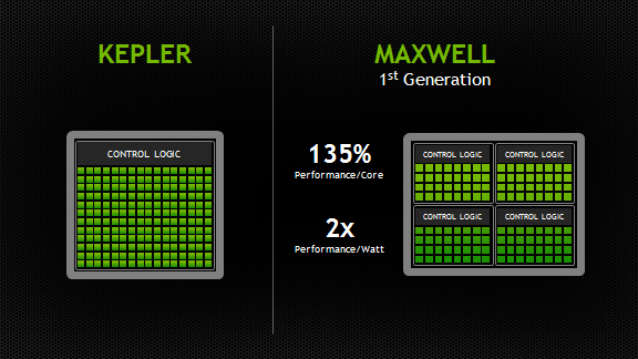
The introduction this week of NVIDIA’s first-generation “Maxwell” GPUs is a very exciting moment for GPU computing. These first Maxwell products, such as the GeForce GTX 750 Ti, are based on the GM107 GPU and are designed for use in low-power environments such as notebooks and small form factor computers. What is exciting about this announcement for HPC and other GPU computing developers is the great leap in energy efficiency that Maxwell provides: nearly twice that of the Kepler GPU architecture.
This post will tell you five things that you need to know about Maxwell as a GPU computing programmer, including high-level benefits of the architecture, specifics of the new Maxwell multiprocessor, guidance on tuning and pointers to more resources.
As with SMX, each SMM has four warp schedulers, but unlike SMX, all core SMM functional units are assigned to a particular scheduler, with no shared units. The power-of-two number of CUDA Cores per partition simplifies scheduling, as each of SMM’s warp schedulers issue to a dedicated set of CUDA Cores equal to the warp width. Each warp scheduler still has the flexibility to dual-issue (such as issuing a math operation to a CUDA Core in the same cycle as a memory
operation to a load/store unit), but single-issue is now sufficient to fully utilize all CUDA Cores.
similar in many respects to the Kepler architecture’s SMX, with key
enhancements geared toward improving efficiency without requiring
significant increases in available parallelism per SM from the
application. The register file size and the maximum number of concurrent
warps in SMM are the same as in SMX (64k 32-bit registers and 64 warps,
respectively), as is the maximum number of registers per thread (255).
However the maximum number of active thread blocks per multiprocessor
has been doubled over SMX to 32, which should result in an automatic
occupancy improvement for kernels that use small thread blocks of 64 or
fewer threads (assuming available registers and shared memory are not
the occupancy limiter). Table 1 provides a comparison between key
characteristics of Maxwell GM107 and its predecessor Kepler GK107.
instruction latencies have been significantly reduced. Because occupancy
(which translates to available warp-level parallelism) is the same or
better on SMM than on SMX, these reduced latencies improve utilization
and throughput.
Table 1. A Comparison of Maxwell GM107 to Kepler GK107
dedicated shared memory per SM—unlike Fermi and Kepler, which
partitioned the 64KB of memory between L1 cache and shared memory. The
per-thread-block limit remains 48KB on Maxwell, but the increase in
total available shared memory can lead to occupancy
improvements. Dedicated shared memory is made possible in Maxwell by
combining the functionality of the L1 and texture caches into a single
unit.
integers and native shared memory 32-bit and 64-bit compare-and-swap
(CAS), which can be used to implement other atomic functions. In
contrast, the Fermi and Kepler architectures implemented shared memory
atomics using a lock/update/unlock pattern that could be expensive in
the presence of high contention for updates to particular locations in
shared memory.
Parallelism, which allows the GPU to create additional work for itself. A
programming model enhancement leveraging this feature was introduced in
CUDA 5.0 to enable threads running on GK110 to launch additional
kernels onto the same GPU.
SMM brings Dynamic Parallelism into the mainstream by supporting it
across the product line, even in lower-power chips such as GM107. This
will benefit developers, because it means that applications will no
longer need special-case algorithm implementations for high-end GPUs
that differ from those usable in more power constrained environments.
This post will tell you five things that you need to know about Maxwell as a GPU computing programmer, including high-level benefits of the architecture, specifics of the new Maxwell multiprocessor, guidance on tuning and pointers to more resources.
1. The Heart of Maxwell: More Efficient Multiprocessors
Maxwell introduces an all-new design for the Streaming Multiprocessor (SM) that dramatically improves power efficiency. Although the Kepler SMX design was extremely efficient for its generation, through its development NVIDIA’s GPU architects saw an opportunity for another big leap forward in architectural efficiency; the Maxwell SM is the realization of that vision. Improvements to control logic partitioning, workload balancing, clock-gating granularity, instruction scheduling, number of instructions issued per clock cycle, and many other enhancements allow the Maxwell SM (also called “SMM”) to far exceed Kepler SMX efficiency. The new Maxwell SM architecture enabled us to increase the number of SMs to five in GM107, compared to two in GK107, with only a 25% increase in die area.Improved Instruction Scheduling
The number of CUDA Cores per SM has been reduced to a power of two, however with Maxwell’s improved execution efficiency, performance per SM is usually within 10% of Kepler performance, and the improved area efficiency of the SM means CUDA cores per GPU will be substantially higher versus comparable Fermi or Kepler chips. The Maxwell SM retains the same number of instruction issue slots per clock and reduces arithmetic latencies compared to the Kepler design.As with SMX, each SMM has four warp schedulers, but unlike SMX, all core SMM functional units are assigned to a particular scheduler, with no shared units. The power-of-two number of CUDA Cores per partition simplifies scheduling, as each of SMM’s warp schedulers issue to a dedicated set of CUDA Cores equal to the warp width. Each warp scheduler still has the flexibility to dual-issue (such as issuing a math operation to a CUDA Core in the same cycle as a memory
operation to a load/store unit), but single-issue is now sufficient to fully utilize all CUDA Cores.
Increased Occupancy for Existing Code
In terms of CUDA compute capability, Maxwell’s SM is CC 5.0. SMM issimilar in many respects to the Kepler architecture’s SMX, with key
enhancements geared toward improving efficiency without requiring
significant increases in available parallelism per SM from the
application. The register file size and the maximum number of concurrent
warps in SMM are the same as in SMX (64k 32-bit registers and 64 warps,
respectively), as is the maximum number of registers per thread (255).
However the maximum number of active thread blocks per multiprocessor
has been doubled over SMX to 32, which should result in an automatic
occupancy improvement for kernels that use small thread blocks of 64 or
fewer threads (assuming available registers and shared memory are not
the occupancy limiter). Table 1 provides a comparison between key
characteristics of Maxwell GM107 and its predecessor Kepler GK107.
Reduced Arithmetic Instruction Latency
Another major improvement of SMM is that dependent arithmeticinstruction latencies have been significantly reduced. Because occupancy
(which translates to available warp-level parallelism) is the same or
better on SMM than on SMX, these reduced latencies improve utilization
and throughput.
| GPU | GK107 (Kepler) | GM107 (Maxwell) |
| CUDA Cores | 384 | 640 |
| Base Clock | 1058 MHz | 1020 MHz |
| GPU Boost Clock | N/A | 1085 MHz |
| GFLOP/s | 812.5 | 1305.6 |
| Compute Capability | 3.0 | 5.0 |
| Shared Memory / SM | 16KB / 48 KB | 64 KB |
| Register File Size / SM | 256 KB | 256 KB |
| Active Blocks / SM | 16 | 32 |
| Memory Clock | 5000 MHz | 5400 MHz |
| Memory Bandwidth | 80 GB/s | 86.4 GB/s |
| L2 Cache Size | 256 KB | 2048 KB |
| TDP | 64W | 60W |
| Transistors | 1.3 Billion | 1.87 Billion |
| Die Size | 118 mm2 | 148 mm2 |
| Manufactoring Process | 28 nm | 28 nm |
2. Larger, Dedicated Shared Memory
A significant improvement in SMM is that it provides 64KB ofdedicated shared memory per SM—unlike Fermi and Kepler, which
partitioned the 64KB of memory between L1 cache and shared memory. The
per-thread-block limit remains 48KB on Maxwell, but the increase in
total available shared memory can lead to occupancy
improvements. Dedicated shared memory is made possible in Maxwell by
combining the functionality of the L1 and texture caches into a single
unit.
3. Fast Shared Memory Atomics
Maxwell provides native shared memory atomic operations for 32-bitintegers and native shared memory 32-bit and 64-bit compare-and-swap
(CAS), which can be used to implement other atomic functions. In
contrast, the Fermi and Kepler architectures implemented shared memory
atomics using a lock/update/unlock pattern that could be expensive in
the presence of high contention for updates to particular locations in
shared memory.
4. Support for Dynamic Parallelism
Kepler GK110 introduced a new architectural feature called DynamicParallelism, which allows the GPU to create additional work for itself. A
programming model enhancement leveraging this feature was introduced in
CUDA 5.0 to enable threads running on GK110 to launch additional
kernels onto the same GPU.
SMM brings Dynamic Parallelism into the mainstream by supporting it
across the product line, even in lower-power chips such as GM107. This
will benefit developers, because it means that applications will no
longer need special-case algorithm implementations for high-end GPUs
that differ from those usable in more power constrained environments.
5. Learn More about Programming Maxwell
For more architecture details and guidance on optimizing your code for Maxwell, I encourage you to check out the Maxwell Tuning Guide and Maxwell Compatibility Guide, which are available now to CUDA Registered Developers.
相关文章推荐
- 修改VirtualBox虚拟机默认存储路径及虚拟机迁移方法
- Servlet 共享变量
- 2016.3.7__HTML 基础_第一天
- Need to include strsafe.h after tchar.h
- 十步轻松搞定IIS+PHP环境搭建
- codeforces 617E. XOR and Favorite Number 莫队
- 通用程序自动更新升级
- Swift学习 字符串的操作
- BP算法的回归
- asp.net框架
- JAVA——java常见的异常大集合
- C++上机报告(二)
- 上机实验2222
- EIP & EBP & ESP
- SQL读书笔记(十二) 插入数据
- 2016春季练习——贪心
- 导出word 服务器报错修正
- c++第一次实验
- 播放视频框架Vitamio导包及应用总结
- C++第一次上机实验报告-1