主板芯片和内存MAP, Motherboard Chipsets and the Memory Map
2011-09-04 15:26
489 查看
原文在:http://duartes.org/gustavo/blog/post/motherboard-chipsets-memory-map
作者对系统的内部实现很感兴趣并实现过很多kernel module。准备写一些列的文章。本篇是他所写的第一篇。我保留大部分原来的英文。并按照自己的理解进行了翻译和批注:)(括号中的话是我自己的一些旁注)
This first post describes the layout of modern Intel-based motherboards, how the CPU accesses memory and the system memory map.
第一篇描述了现代Intel-based的主板上CPU是如何访问内存以及系统内存的布局。(我更喜欢arm系列的嵌入式设备,希望之后我能有能力仿造作者的足迹,提供相对应的arm architecture的开发板的相关文章)
To start off let’s take a look at how an Intel computer is wired up nowadays. The diagram below shows the main components in a motherboard and dubious color taste:
首先, 让我们看一下intel的电脑中的各个硬件模块是如何相互关联的(不知道是否跟最新的I3/I5/I7还一致,希望对intel系列了解的同学能够补充)。下图显示了最主要的一些组件:(关于南北桥各自所经常连接的模块在《Essential
Linux Device Drivers》中对每一中设备进行描述时都会提到它是与哪一个桥相连。其中只要知道显卡和内存是连在北桥的,其它都在南桥就行了)
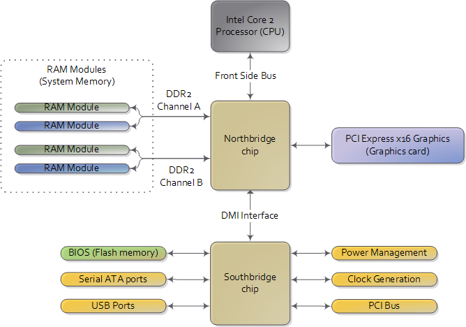
Diagram for modern motherboard. The northbridge and southbridge make up the chipset.
As you look at this, the crucial thing to keep in mind is that the CPU doesn’t really know anything about what it’s connected to. It talks to the outside world through its pins but it doesn’t care what that outside world is.
It might be a motherboard in a computer but it could be a toaster, network router, brain implant, or CPU test bench. There are three main ways by which the CPU and the outside communicate: memory address space, I/O address space, and interrupts. We only worry
about motherboards and memory for now.
就像你所看到的,请您一定记住,CPU是完全不知道它自己所能连接到的其它设备。 它只是通过它的pins来与外界交互,但是完全不在乎外面的世界是什么样的。 它可能处在一个普通的主板上,也可能处于一个烤面包机,交换机,brain implant, 或者是CPU的测试板卡里。有三种主要的方式被CPU利用来与外界交互:内存地址空间, I/O地址空间(大部分嵌入式体系结构没有相关概念,而是统一到内存地址空间当中去了),中断。目前我们只关注主板和
In a motherboard the CPU’s gateway to the world is the front-side bus connecting it to the northbridge. Whenever the CPU needs to read or write memory it does so via this bus. It uses some pins to transmit the physical memory
address it wants to write or read, while other pins send the value to be written or receive the value being read. An Intel Core 2 QX6600 has 33 pins to transmit the physical memory address (so there are 233 choices of memory locations) and 64 pins
to send or receive data (so data is transmitted in a 64-bit data path, or 8-byte chunks). This allows the CPU to physically address 64 gigabytes of memory (233 locations * 8 bytes) although most chipsets only handle up to 8 gigs of RAM.
主板上的CPU通过前端的bus连接到北桥来作为它通向世界的gateway(SoC上就没这南/北桥的概念喽)。 无论什么时候CPU需要读写内存都需要通过该bus。 它通过一些引脚来传输它所想要读写的物理地地而通过另外一些引脚来获得读/写到的值。 Intel Core 2 QX6600有33个引脚用来传输物理地址(所以有233 个内存位置可供选择)并且有64个引脚用来发或者接收数据(所以可以使用64-bit
data path)。这就允许CPU可以寻址64 gigabytes的内存(233 locations * 8 bytes),但是大部分芯片组只处理8 gigs的内存。
Now comes the rub. We’re used to thinking of memory only in terms of RAM, the stuff programs read from and write to all the time. And indeed most of the memory requests from the processor are routed to RAM modules by the northbridge.
But not all of them. Physical memory addresses are also used for communication with assorted devices on the motherboard (this communication is calledmemory-mapped I/O). These devices include video
cards, most PCI cards (say, a scanner or SCSI card), and also theflash memory that stores the BIOS.
现在让我们来看看内存, 这里只考虑RAM, 从始至终的被程序用来读和写数据。并且大部分的内存需求都是处理器通过北桥来传递到内存的。但是,事无绝对。物理内存地址也被CPU用来和主板上的其它设备交互(这些交互就叫做memory-mapped I/O). 这些设备包括显卡,大多数的PCI卡(比如,扫描仪或者SCSI卡),还有保存BIOS的flash memory.
When the northbridge receives a physical memory request it decides where to route it: should it go to RAM? Video card maybe? This routing is decided via the memory address map. For each region of physical memory addresses, the
memory map knows the device that owns that region. The bulk of the addresses are mapped to RAM, but when they aren’t the memory map tells the chipset which device should service requests for those addresses. This mapping of memory addresses away from RAM modules
causes the classic hole in PC memory between 640KB and 1MB. A bigger hole arises when memory addresses are reserved for video cards and PCI devices. This is why 32-bit OSes haveproblems using 4 gigs of RAM.
In Linux the file/proc/iomem neatly lists these address range mappings. The diagram below shows a typical memory map for the first 4 gigs of physical memory addresses in an Intel PC:
当北桥接到一个对物理内存的请求时,它决定该请求应该导向到哪里:是去RAM呢?或者是显卡?这种route通过memory address map来决定。对于每个物理内存地址的区域,memory map知道哪一块区域被哪一个设备所拥有。 大部分的地址都被RAM所map,但是当它们不是memory map的时候,需要告诉芯片组哪一个设备负责响应对该地址的请求。在PC的内存地址中,从640KB到1MB的空间被称为是经典hole,它不是留给RAM来map。会有一个大的内存区域(hole)是留给显卡和PCI设备来map的。
这就是为什么32位的操作系统没办法使用所有4G的内存。在linux的/proc/iomem中清晰的给出了一个关于所有内存区间map关系的列表。 下图显示了一个典型inte lPC的4G物理内存地址的memory map:
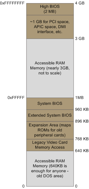
Memory layout for the first 4 gigabytes in an Intel system.
Actual addresses and ranges depend on the specific motherboard and devices present in the computer, but most Core 2 systems are pretty close to the above. All of the brown regions are mapped away from RAM. Remember that these
are physical addresses that are used on the motherboard buses. Inside the CPU (for example, in the programs we run and write), the memory addresses are logical and they must be translated by the CPU into a physical address
before memory is accessed on the bus.
实际的地址和区域依赖与特定的主板和主板上的设备,但是,大部分的core 2系统都跟上面的图形类似。 所有褐色的区域就是用来给RAM mapped。请记住这些物理地址都是被在主板的总线上使用。 在CPU内部(例如,程序中的读和写),那些内存地址都是逻辑上的,它们必须被CPU所翻译成物理地址然后才能在总线上去访问该内存。
The rules for translation of logical addresses into physical addresses are complex and they depend on the mode in which the CPU is running (real mode, 32-bit protected mode, and 64-bit protected mode). Regardless of
the translation mechanism, the CPU mode determines how much physical memory can be accessed. For example, if the CPU is running in 32-bit mode, then it is only capable of physically addressing 4 GB (well, there is an exception called physical
address extension, but ignore it for now). Since the top 1 GB or so of physical addresses are mapped to motherboard devices the CPU can effectively use only ~3 GB of RAM (sometimes less – I have a Vista machine where only 2.4 GB are usable). If the CPU
is in real mode, then it can only address 1megabyte of physical RAM (this is the only mode early Intel processors were capable of). On the other hand, a CPU running in 64-bit mode can physically
access 64GB (few chipsets support that much RAM though). In 64-bit mode it is possible to use physical addresses above the total RAM in the system to access the RAM regions that correspond to physical addresses stolen by motherboard devices. This is called reclaiming
memory and it’s done with help from the chipset.
逻辑地址翻译为物理地址的规则是复杂的并且依赖与CPU运行的状态(实模式,32位保护模式,64位保护模式)。 无论什么样的翻译机制, CPU的模式决定了多少物理地址能够被访问。 例如, 如果CPU运行在32位模式下, 那么只能够最多访问到4G的物理地址(这里我们忽略PAE机制所做的扩展)。 因为由于最上面的1GB和那些被其它设备所占用的地址外,CPU只能有效的寻址大约3GB的内存。 如果CPU在实模式, 那么它只能够寻址1M的物理内存(这是因为早期的intel处理器的限制)。
另一方面, 运行在64位模式下的CPU能够寻址64GB(一些芯片组可以支持更大的RAM)。 在64位模式下, 它能够使用超过系统所有的RAM的物理地址空间,包括那些被其它设备所占用的地址。 这叫做reclaiming memory,这需要芯片组的帮组。
That’s all the memory we need for the next post, which describes the boot process from power up until the boot loader is about to jump into the kernel. If you’d like to learn more about this stuff, I highly recommend the Intel
manuals. I’m big into primary sources overall, but the Intel manuals in particular are well written and accurate. Here are some:
这就是我们为下一个专题所做的关于内存的介绍, 下一个专题要描述从上电到boot loader到启动内核的过程。 这里我推荐intel manuals给想要知道更多细节的朋友。 比如下面这些:
Datasheet for Intel G35 Chipset documents a representative chipset for Core 2 processors. This is the main source for this post.
Datasheet for Intel Core 2 Quad-Core Q6000 Sequence is a processor datasheet. It documents each pin in the processor (there aren’t that many actually,
and after you group them there’s really not a lot to it). Fascinating stuff, though some bits are arcane.
The
Intel Software Developer’s Manuals are outstanding. Far from arcane, they explain beautifully all sorts of things about the architecture. Volumes 1 and 3A have the good stuff (don’t be put off by the name, the “volumes” are small and you can read selectively).
Pádraig Brady
suggested that I link to Ulrich Drepper’s excellent paper on memory. It’s
great stuff. I was waiting to link to it in a post about memory, but the more the merrier.
What Every Programmer Should Know About Memory
准备仔细阅读下,希望能有时间整理并翻译下来。
作者对系统的内部实现很感兴趣并实现过很多kernel module。准备写一些列的文章。本篇是他所写的第一篇。我保留大部分原来的英文。并按照自己的理解进行了翻译和批注:)(括号中的话是我自己的一些旁注)
This first post describes the layout of modern Intel-based motherboards, how the CPU accesses memory and the system memory map.
第一篇描述了现代Intel-based的主板上CPU是如何访问内存以及系统内存的布局。(我更喜欢arm系列的嵌入式设备,希望之后我能有能力仿造作者的足迹,提供相对应的arm architecture的开发板的相关文章)
To start off let’s take a look at how an Intel computer is wired up nowadays. The diagram below shows the main components in a motherboard and dubious color taste:
首先, 让我们看一下intel的电脑中的各个硬件模块是如何相互关联的(不知道是否跟最新的I3/I5/I7还一致,希望对intel系列了解的同学能够补充)。下图显示了最主要的一些组件:(关于南北桥各自所经常连接的模块在《Essential
Linux Device Drivers》中对每一中设备进行描述时都会提到它是与哪一个桥相连。其中只要知道显卡和内存是连在北桥的,其它都在南桥就行了)
Diagram for modern motherboard. The northbridge and southbridge make up the chipset.
As you look at this, the crucial thing to keep in mind is that the CPU doesn’t really know anything about what it’s connected to. It talks to the outside world through its pins but it doesn’t care what that outside world is.
It might be a motherboard in a computer but it could be a toaster, network router, brain implant, or CPU test bench. There are three main ways by which the CPU and the outside communicate: memory address space, I/O address space, and interrupts. We only worry
about motherboards and memory for now.
就像你所看到的,请您一定记住,CPU是完全不知道它自己所能连接到的其它设备。 它只是通过它的pins来与外界交互,但是完全不在乎外面的世界是什么样的。 它可能处在一个普通的主板上,也可能处于一个烤面包机,交换机,brain implant, 或者是CPU的测试板卡里。有三种主要的方式被CPU利用来与外界交互:内存地址空间, I/O地址空间(大部分嵌入式体系结构没有相关概念,而是统一到内存地址空间当中去了),中断。目前我们只关注主板和
In a motherboard the CPU’s gateway to the world is the front-side bus connecting it to the northbridge. Whenever the CPU needs to read or write memory it does so via this bus. It uses some pins to transmit the physical memory
address it wants to write or read, while other pins send the value to be written or receive the value being read. An Intel Core 2 QX6600 has 33 pins to transmit the physical memory address (so there are 233 choices of memory locations) and 64 pins
to send or receive data (so data is transmitted in a 64-bit data path, or 8-byte chunks). This allows the CPU to physically address 64 gigabytes of memory (233 locations * 8 bytes) although most chipsets only handle up to 8 gigs of RAM.
主板上的CPU通过前端的bus连接到北桥来作为它通向世界的gateway(SoC上就没这南/北桥的概念喽)。 无论什么时候CPU需要读写内存都需要通过该bus。 它通过一些引脚来传输它所想要读写的物理地地而通过另外一些引脚来获得读/写到的值。 Intel Core 2 QX6600有33个引脚用来传输物理地址(所以有233 个内存位置可供选择)并且有64个引脚用来发或者接收数据(所以可以使用64-bit
data path)。这就允许CPU可以寻址64 gigabytes的内存(233 locations * 8 bytes),但是大部分芯片组只处理8 gigs的内存。
Now comes the rub. We’re used to thinking of memory only in terms of RAM, the stuff programs read from and write to all the time. And indeed most of the memory requests from the processor are routed to RAM modules by the northbridge.
But not all of them. Physical memory addresses are also used for communication with assorted devices on the motherboard (this communication is calledmemory-mapped I/O). These devices include video
cards, most PCI cards (say, a scanner or SCSI card), and also theflash memory that stores the BIOS.
现在让我们来看看内存, 这里只考虑RAM, 从始至终的被程序用来读和写数据。并且大部分的内存需求都是处理器通过北桥来传递到内存的。但是,事无绝对。物理内存地址也被CPU用来和主板上的其它设备交互(这些交互就叫做memory-mapped I/O). 这些设备包括显卡,大多数的PCI卡(比如,扫描仪或者SCSI卡),还有保存BIOS的flash memory.
When the northbridge receives a physical memory request it decides where to route it: should it go to RAM? Video card maybe? This routing is decided via the memory address map. For each region of physical memory addresses, the
memory map knows the device that owns that region. The bulk of the addresses are mapped to RAM, but when they aren’t the memory map tells the chipset which device should service requests for those addresses. This mapping of memory addresses away from RAM modules
causes the classic hole in PC memory between 640KB and 1MB. A bigger hole arises when memory addresses are reserved for video cards and PCI devices. This is why 32-bit OSes haveproblems using 4 gigs of RAM.
In Linux the file/proc/iomem neatly lists these address range mappings. The diagram below shows a typical memory map for the first 4 gigs of physical memory addresses in an Intel PC:
当北桥接到一个对物理内存的请求时,它决定该请求应该导向到哪里:是去RAM呢?或者是显卡?这种route通过memory address map来决定。对于每个物理内存地址的区域,memory map知道哪一块区域被哪一个设备所拥有。 大部分的地址都被RAM所map,但是当它们不是memory map的时候,需要告诉芯片组哪一个设备负责响应对该地址的请求。在PC的内存地址中,从640KB到1MB的空间被称为是经典hole,它不是留给RAM来map。会有一个大的内存区域(hole)是留给显卡和PCI设备来map的。
这就是为什么32位的操作系统没办法使用所有4G的内存。在linux的/proc/iomem中清晰的给出了一个关于所有内存区间map关系的列表。 下图显示了一个典型inte lPC的4G物理内存地址的memory map:
Memory layout for the first 4 gigabytes in an Intel system.
Actual addresses and ranges depend on the specific motherboard and devices present in the computer, but most Core 2 systems are pretty close to the above. All of the brown regions are mapped away from RAM. Remember that these
are physical addresses that are used on the motherboard buses. Inside the CPU (for example, in the programs we run and write), the memory addresses are logical and they must be translated by the CPU into a physical address
before memory is accessed on the bus.
实际的地址和区域依赖与特定的主板和主板上的设备,但是,大部分的core 2系统都跟上面的图形类似。 所有褐色的区域就是用来给RAM mapped。请记住这些物理地址都是被在主板的总线上使用。 在CPU内部(例如,程序中的读和写),那些内存地址都是逻辑上的,它们必须被CPU所翻译成物理地址然后才能在总线上去访问该内存。
The rules for translation of logical addresses into physical addresses are complex and they depend on the mode in which the CPU is running (real mode, 32-bit protected mode, and 64-bit protected mode). Regardless of
the translation mechanism, the CPU mode determines how much physical memory can be accessed. For example, if the CPU is running in 32-bit mode, then it is only capable of physically addressing 4 GB (well, there is an exception called physical
address extension, but ignore it for now). Since the top 1 GB or so of physical addresses are mapped to motherboard devices the CPU can effectively use only ~3 GB of RAM (sometimes less – I have a Vista machine where only 2.4 GB are usable). If the CPU
is in real mode, then it can only address 1megabyte of physical RAM (this is the only mode early Intel processors were capable of). On the other hand, a CPU running in 64-bit mode can physically
access 64GB (few chipsets support that much RAM though). In 64-bit mode it is possible to use physical addresses above the total RAM in the system to access the RAM regions that correspond to physical addresses stolen by motherboard devices. This is called reclaiming
memory and it’s done with help from the chipset.
逻辑地址翻译为物理地址的规则是复杂的并且依赖与CPU运行的状态(实模式,32位保护模式,64位保护模式)。 无论什么样的翻译机制, CPU的模式决定了多少物理地址能够被访问。 例如, 如果CPU运行在32位模式下, 那么只能够最多访问到4G的物理地址(这里我们忽略PAE机制所做的扩展)。 因为由于最上面的1GB和那些被其它设备所占用的地址外,CPU只能有效的寻址大约3GB的内存。 如果CPU在实模式, 那么它只能够寻址1M的物理内存(这是因为早期的intel处理器的限制)。
另一方面, 运行在64位模式下的CPU能够寻址64GB(一些芯片组可以支持更大的RAM)。 在64位模式下, 它能够使用超过系统所有的RAM的物理地址空间,包括那些被其它设备所占用的地址。 这叫做reclaiming memory,这需要芯片组的帮组。
That’s all the memory we need for the next post, which describes the boot process from power up until the boot loader is about to jump into the kernel. If you’d like to learn more about this stuff, I highly recommend the Intel
manuals. I’m big into primary sources overall, but the Intel manuals in particular are well written and accurate. Here are some:
这就是我们为下一个专题所做的关于内存的介绍, 下一个专题要描述从上电到boot loader到启动内核的过程。 这里我推荐intel manuals给想要知道更多细节的朋友。 比如下面这些:
Datasheet for Intel G35 Chipset documents a representative chipset for Core 2 processors. This is the main source for this post.
Datasheet for Intel Core 2 Quad-Core Q6000 Sequence is a processor datasheet. It documents each pin in the processor (there aren’t that many actually,
and after you group them there’s really not a lot to it). Fascinating stuff, though some bits are arcane.
The
Intel Software Developer’s Manuals are outstanding. Far from arcane, they explain beautifully all sorts of things about the architecture. Volumes 1 and 3A have the good stuff (don’t be put off by the name, the “volumes” are small and you can read selectively).
Pádraig Brady
suggested that I link to Ulrich Drepper’s excellent paper on memory. It’s
great stuff. I was waiting to link to it in a post about memory, but the more the merrier.
What Every Programmer Should Know About Memory
准备仔细阅读下,希望能有时间整理并翻译下来。

相关文章推荐
- Motherboard Chipsets and the Memory Map -- 主板芯片和内存映射
- 底板芯片组与内存映射(Motherboard Chipsets and the Memory Map) 【转】
- Motherboard Chipsets and the Memory Map
- Motherboard Chipsets and the Memory Map
- Motherboard Chipsets and the Memory Map
- Motherboard Chipsets and the Memory Map
- 工作于内存和文件之间的页缓存, Page Cache, the Affair Between Memory and Files
- 工作于内存和文件之间的页缓存, Page Cache, the Affair Between Memory and Files
- 内存分布和栈空间---Memory Layout And The Stack
- 工作于内存和文件之间的页缓存, Page Cache, the Affair Between Memory and Files
- HDOJ.1029 Ignatius and the Princess IV(map)
- Page Cache, the Affair Between Memory and Files
- Boost.Interprocess使用手册翻译之八:分配器,容器和内存分配算法(Allocators, containers and memory allocation algorithms)
- The Java™ Tutorials — Concurrency :Memory Consistency Errors 内存一致性错误
- When bootstub get control, the memory map in DRAM is like
- STM32学习笔记(2):存储器映射和存储器重映射(Memory Map and Memory Remap)
- 释放内存free()错误:CRT detected that the application wrote to memory after end of heap buffer:内存访问违规
- [转]Installing, Configuring and Using Windows Server AppFabric and the "Velocity" Memory Cache in 10 minutes
- Platform Road Map for the MATLAB and Simulink Product Families
- Cracking the Coding Interview-ch11 | System Design and Memory Limits